

In this post we learn how to make simple and easy hobby circuits using any NAND gate IC such as IC 4011, IC 7400 or IC 4093
What is a Schmitt Trigger
A Schmitt trigger is a quite simple kind of circuit, but it is amongst the most successful of all electronic building blocks and is largely utilised in home constructor projects. Basically a Schmitt trigger is a circuit which could simply have one of two stable states (high or low) at its output.
Which of these states the output assumes is dependent upon perhaps the input of the circuit is above or below a specific threshold voltage.
Most Schmitt trigger circuits have a degree of hysteresis, and so the threshold voltage at which the output goes high is above the threshold voltage at which it returns to the low state.
In many hobby applications this is a remarkably advisable feature, and in couple of it is totally necessary, but it is normally essential to possess at least a small degree of hysteresis as in any other case the circuit would usually turn out to be unstable with the input at or very close to the threshold voltage. Hence hysteresis is normally employed whether it is necessary to the basic operating principle of the circuit or not.
CMOS Schmitt trigger I.C.s are obtainable, and the 4093 quad Schmitt trigger is one illustration. On the other hand, generally in most applications merely a single Schmitt trigger is needed, and it is more affordable to connect a number of inverters to form the circuit than it is to employ a special I.C. (which are not as low-cost as simple gates). Either one or both of the unused inverters can occasionally be usefully utilized in a few other portion of the circuit.
1) Simple CMOS Schmitt Trigger Circuit
There are numerous methods for linking gates to form a Schmitt trigger circuit, and the technique displayed in mentioned in the below diagram, is among the most most straightforward. In this article the input of inverter 1 is attached to ground by way of R1, and so the output of this inverter is high. The output of inverter 2 will as a result be low.


If a positive input signal is currently placed on the circuit this will likely take the input of inverter 1 positive, but it won't have any kind of impact on the circuit apart from this unless the input signal reaches an amplitude which is equal to the transfer voltage of inverter 1.
During these moments, the output of inverter 1 will swing down towards the negative supply rail voltage, and this will result in the output of inverter 2 to begin to go high. As it does so it feeds a positive voltage to the input of inverter 1 by way of R2, and this leads to the output of inverter 1 to go more negative.
Thus as a result sends the output of inverter 2 more positive. This particular leads to a further positive voltage to be fed to inverter 1 input by means of R2, and this regenerative action will proceed prior to the output of the circuit is completely positive.
In procedure this all takes place extremely rapidly, and virtually the moment the input voltage reaches the transfer voltage of inverter 1, the output assumes the high state.
If the input signal now starts to swing back towards the negative supply rail, a point will obviously be reached where the input of inverter 1 is obtained below the transfer voltage, and the output will begin to swing negative. A regenerative circuit action will likely then once more occur and the output will soon go completely low.
Hysteresis is presented through the fact that as soon as the output has gone high, the voltage by means of R2 is added to the input signal. This implies that the input signal must work good below the transfer voltage prior to the circuit will resume its original state. The circuit will not normalise till the voltage from the output plus the input signal voltage equals a total which is less than the transfer voltage of inverter 1.
This simple circuit has many functions, and it can, for instance, be applied to generate a squarewave output from a sine or triangular input waveform. It can also be employed to speed up a gradually rising or falling waveform, and it is often essential to do this when using logic devices.
This is due to the fact that many logic devices will not likely perform dependably unless they are managed by a quick rising waveform, and CMOS counters and flip flop for instance, must be powered by an input signal possessing a risetime of 5 micro -seconds or less.
2) Light Detector Circuit
Schmitt triggers are not only employed in A.C. applications, and are commonly used in D.C. circuitry. In this particular kind of application it is generally the role of the circuit to make certain a specific output state is obtained, with no advanced ones being possible.
An illustration of this is the very simple light detector hobby circuit which is demonstrated below. This kind of circuit is employed to close a set of relay contacts when the light level falling on a photocell surpasses a particular level. Such devices works extremely well in burglar alarms and for a number of other requirements.

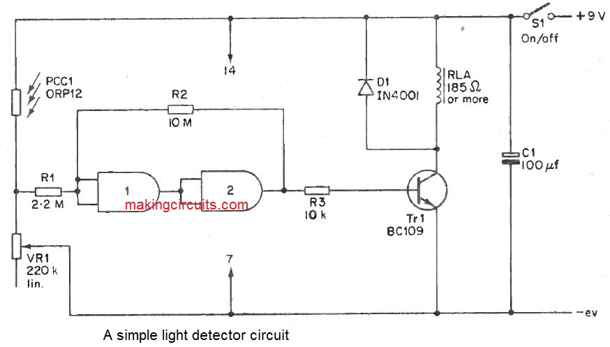
It is almost always essential for the unit to draw a very low standby current so that economic battery procedure is feasible. In the above a simple light detector circuit , the Schmitt trigger helps to ensure that this is certainly obtained. VR1 is altered so that the output of the Schmitt trigger circuit is usually low, and no major base current is delivered to Tr1. This transistor is for that reason cut off and the relay is simply not triggered.
When the light level falling on PCC1 surpasses a particular threshold level, the resistance of this cell will have dropped to a low enough level to cause the voltage at the junction of VR1 and PCC1 to rise above the trigger voltage of the Schmitt trigger. Its output will soon go to the high state and Tr1 will switch on. The relay will then be activated.
Under regular circumstances the Schmitt trigger and the output transistor draw no current, and the only supply current which flows is the small current by means of PCC1 and VR1. The circuit would certainly continue to function if the trigger circuit and R3 were to be avoided, with the junction of PCC1 and VR1 then being attached direct to Tr1 base.
On the other hand, with the circuit in the normal or off state it might be pretty simple for a small base current to be fed to Tr1. This would cause it to draw a substantial collector current which despite the fact that too small to activate the relay, could discharge the batteries over a time frame.
3) Darkness Detector Circuit
In many applications it is essential to possess a circuit which functions a relay when the light level goes below a particular level, instead of when it goes above a particular level.
It is quite simple to transform from the above diagram a simple light detector circuit to achieve this and there are a number of methods for performing it. Most probably the most easy one is simply to transpose VR1 and PCC1. The voltage at the junction of these two devices will then rise with decreasing light level, and the needed circuit action is therefore presented.
4) Latching Version Circuit
In alarm circuits and several other hobby applications it is essential to experience a circuit which will continue to be on as soon as it has been activated. It is an simple matter to make changes in the above a simple light detector circuit diagram to deliver latching, and the modified circuit diagram is found in below :-

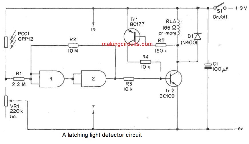
This works in precisely the same technique as the original circuit till the relay is activated. Then the voltage across the relay, which has been formerly zero, increases to many volts, and a base current is delivered to Tr1 by means of current reducing resistor R5. This turns Tr1 on, and a base current will be delivered to Tr2 via Tr1 emitter and collector and current limiting resistor R4.
Even if the output of the Schmitt trigger now results to the low state,
Tr2 is definitely not turned off as it will still be obtaining a base current from Tr1.
The circuit as a result latches in the on state as soon as it has been activated, with Tr1 and Tr2 putting together a sort of thyristor action. Just like the above circuit a simple light detector circuit diagram, this circuit can be developed as a darkness detector by swooping over VR1 and PCC1
5) Automatic Parking Light
In applications where a light switch is to be employed to function a low voltage DC. load it is normally feasible to employ a relayless circuit. An automatic parking light for a car is one this kind of illustration, and a appropriate circuit is demonstrated here below.

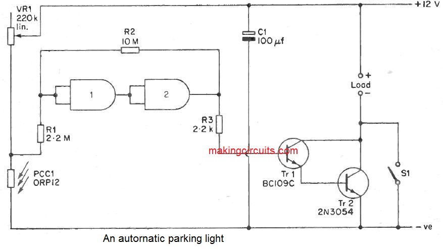
In this article the circuit is triggered as soon as the light level drops below a level which in turn causes the voltage at the junction of VR1 and PCC1 to surpass the trigger voltage of the Schmitt trigger.
The trigger circuit then offers a base current to a high gain Darlington pair utilizing Tr1 and Tr2. Tr2 is a power transistor which is able to handle the comparatively high current captivated by a parking light. S1 permits the light to be switched on separately of the automatic circuitry.
In this circuit the current usage of the device is of secondary significance since it will be powered from a high capacity car battery. On the other hand, it is certainly appealing to have the lamp switching cleanly from one state to another.
Perhaps less obviously it is very important for the circuit to prevent intermediate output states to be able to illiminate the possibility of damage to Tr2 as a result of overheating.
This might take place if Tr2 was partly switched on with about half the supply voltage being present at its collector, as it would then have to dissipate several watts of power.
This might be overcome simply by using a wide range of heatsinking for Tr2, but it is most likely preferable to utilize a trigger circuit, as Tr2 can then only rest in the hard on or fully off state.
The dissipation in any case can simply be low, as when it is turned hard on very little voltage is generated across it, and when it is turned hard off it passes no substantial current.
It will dissipate a substantial amount of power when it is switched on, and if a high current lamp is being managed a certain amount of heatsinking will be essential, but this would only need to be minimal.
Out of all light switches simply explained it is easy to adjust the circuit through VR1 to generate a switching threshold at nearly every essential light intensity.
6) Touch Switch Circuit
A Schmitt trigger can be employed as the basis of an simple touch switch, where it means that the circuit switches quickly from one state to the other and does not pursue a stable intermediate state. It therefore offers an action which can be nearly the same as a standard mechanical switch.
A simple touch switch circuit is demonstrated in below diagram, and this demonstrates what sort of CMOS Schmitt trigger can be utilized as the basis of a novel home made torch. The circuit has additional feasible functions certainly, and any small D.C. load could be linked instead of the lamp.


Other loads could be managed employing a relay in the collector circuit of Tr1, and if this is completed it will likewise be essential to incorporate a protecting diode within this portion of the circuit.
Procedure of the circuit is quite convenient. The Schmitt trigger is organized so that its input and output tend to be normally in the low situation, and Tr1 is as a result generally cut off. When the touch contacts are bridged by the operator's finger a current will flow from the positive supply rail and by means of R1.
In essence, the skin resistance of the functioning finger and R1 collectively form a potential divider, and supplied the voltage at their particular junction is above the threshold voltage of the Schmitt trigger, this specific circuit will presume the high state at the output.
It then gives a base current to Tr1 which is, in consequence, biased hard on. Power is then available to the lamp that ought to have a current utilization of a maximum of around 100 mA.
When the operator's finger is stripped away from the touch contacts the
Schmitt trigger reverts to its original state and the lamp is turned off.
7) Over Temperature Indicator Circuit
In this particular application it is the purpose of the Schmitt trigger to make sure that an wrong indication is not developed. This is merely a circuit signifies using a lamp any rise in temperature above a preset threshold level. If the triggering were to be left out, then the lamp might start to glow dimly as the temperature approached the threshold level.
This might be puzzling, and if the unit is battery powered it might result in the batteries possessing a extremely short functioning life. The circuit diagram of the unit displays in below diagram.

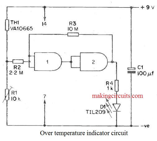
TH1 and R1 are attached as a potential divider at the input of the trigger circuit. TH1 is a negative temperature coefficient thermistor, and its resistance as a result diminishes along with raising temperature.
R1 is adjusted in order that the voltage created by this potential divider reaches the trigger threshold of the Schmitt trigger at the needed threshold temperature. When the output of the Schmitt trigger goes high, power is supplied to the L.E.D. indicator, D1.
When the lamp is in the off state the circuit only utilizes about 1 mA through the supply lines, and this is the power which usually flows through the thermistor and R1.
A reasonable battery life can be acquired simply by using a large capacity battery to power the unit, but in many cases it will probably be better to utilize a small battery and connect a push to create non -locking push button switch in series with the positive supply lead.
The unit will then only consume power when this push switch is controlled. Certainly in a few applications this method of periodic monitoring will not be appropriate, but it is recommended to use it where ever it is useful to do so.
A wide range of threshold temperatures can be supplied by R1, and the actual functioning range of the circuit extends from more than 100 degrees Fahrenheit to less than 0 degrees Fahrenheit. Hence , it is an extremely multipurpose circuit.
It is far from important for the thermistor to be included in the main unit, and there is no reason why it may not be remotely placed from the rest of the unit. Quite a long connecting cable can be utilized amongst the thermistor sensor and the rest of the unit if possible. The unit could thus be applied as a fire alarm for an outbuilding, or in a few related
8) Under Temperature Version Circuit
The over temperature indicator circuit diagram is effortlessly revised to work as an under temperature indicator, and it is simply essential to transpose the positions of R1 and TH1. The circuit could then be employed, for instance, as a frost alarm, and might be used by gardeners or in automotive applications. The operating temperature range is equivalent for the original version of the unit.
By utilizing all four gates of a 4001 or 4011 I.C. it might be possible to generate both versions of the unit employing a single device. The unit might then be adjusted in order that it would reveal any temperature deviation outside two preset limits.
9) Over Temperature Alarm Circuit
This is simply the similar circuit as the over temperature indicator, but the output of the Schmitt trigger is utilized to manage an audible slams circuit instead of an indicator light. The circuit diagram of this unit is found in below diagram.

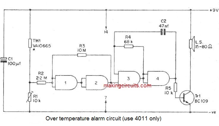
Inverter 3 and inverter 4 are linked as an astable multvibrator which usually works at a frequency of a few hundred Hz. This particular feeds a common emitter amplifier employing Tr1 , and this also subsequently performs a loudspeaker.
The multivibrator is blocked and are unable to work until the output of the Schmitt trigger is high, and the alarm will not as a result sound prior to the circuit continues to be triggered.
The quiescent current and functioning temperature range of this circuit are exactly the same as for the over temperature indicator. The unit can be
transformed into an under temperature alarm by swopping over R1 and
TH1
It is recommended to be aware that this circuit is only going to operate by employing a 4011 I.C., and a 4001 is not really appropriate in this situation.
Providing R1 with the correct adjustment is pretty simple and is the same for this circuit and for the over temperature indicator. The thermistor is heated or cooled to the needed threshold temperature, and then R1 is adjusted for the lowest resistance which in turn causes the indicator lamp to conic on or the alarm to sound, as suitable.
For the under temperature versions the method is significantly a similar, the only change being that R1 needs to be adjusted for the highest resistance which keeps the indicator lamp on or the alarm sounding.
10) Timer with Buzzer Circuit
Two simple timers which offer an audible output at the end of a variable timing period seem to have been included. These circuits were restricted to a maximum timing span of approximately 10 seconds, due to the fact utilizing a longer time constant would result in the tone generator being switched on simply slowly, which may certainly not be sufficient.
The timer circuit demonstrated in below diagram is actually identical to the original one (see the diagram in 0-10 sec. timer circuit) in that it employs an R-C timing network and an astable multivibrator tone generator. On the other hand, rather than the tone generated being fed to the output stage/speaker through an permitting gate,it is fed direct to this arrangement.

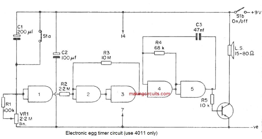
The multivibrator on its own is managed on this situation, via a control voltage which is fed to one input of gate 4. This terminal is usually low and the astable circuit is muted. The output of gate 5 is also usually low with Tr1 being shut down and passing no current. This will be significant, as if it were generally high, Tr1 will be biased on and there would be a very high static current consumption.
Gates 2 and 3 are utilized as the Schmitt trigger, and this has its input fed from an inverter which often has its input fed through the R-C timing network. C1 is the capacitive portion of the timing network and R1 -
VR1 are the resistive part.
S1 a opens once the on/off switch (Sib) is closed, and this begins the timing interval. C1 starts to charge up by means of VR1 and R1 and finally the voltage across R1 and VR1 will fall to the transfer voltage of gate 1. When this occurs, the output voltage of gate 1 will slowly commence to rise.
After a short while its output voltage will achieve the trigger voltage of the Schmitt trigger circuit, and the output of inverter 3 will instantly go higher. This activates the multivibrator and the audible alarm tone is created from the speaker.
Once the unit is turned off, S1 a discharges C1 and the unit is then all set to commence one more timing period when it is switched on yet again.
VR1 permits the length of the timing interval to be varied from less than 30 seconds to more than 6 minutes, and the unit is thus ideal for work with as an egg timer, or indeed for a multitude of purposes in the house. A timer of this sort can be a lot more beneficial compared to one may possibly visualize.
A dial calibrated in minutes ought to be marked around the control knob of VR1, and there is regrettably no fast method of carrying this out. It is a matter of discovering all the calibration points utilizing a procedure for trial and error.
Remember that this particular circuit can simply be developed employing a 4011 IC., as gate 4 must be a NAND type. Truth be known it will require two I.C.s, since five gates are utilized in the circuit and only four are contained in each 4011 I.C.
11) Under Voltage Indicator Circuit
Several pieces of 9 volt battery managed equipment, especially with regards to test equipment, make use of a stabilised supply rail of between 5.6 and 7.5 V.
Failure of the equipment can take place if this voltage will drop below its nominal level as a result of battery ageing, numerous pieces of gear usually do not include any kind of battery check facility. This is often included in this kind of equipment utilizing the basic circuit displayed in below diagram.

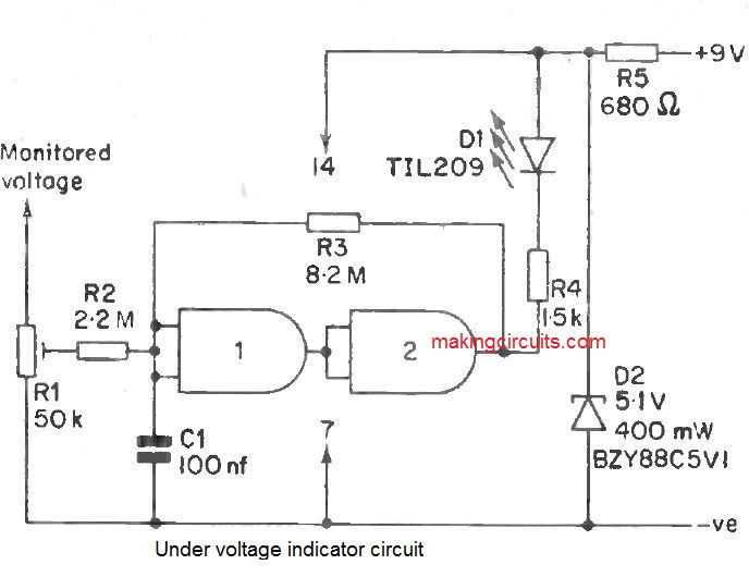
The upper and lower threshold voltages of a CMOS Schmitt trigger are dependant upon the individual properties of the gates used and by the supply rail potential. This circuit is as a result powered from a stabilized supply in order that these voltages are generally not substantially impacted by variations in the supply rail potential. This stabilized potential has been conducted less than that of the monitored voltage for obvious causes.
The two inverters are linked as a simple Schmitt trigger which includes its input fed from the monitored voltage by using a preset potentiometer (R1). R1 is adjusted in order that the Schmitt trigger is usually in the high state, with the voltage at its slider being fractionally higher than the lower threshold voltage of the Schmitt trigger.
An L.E.D. indicator (D1) and current limiting resistor (R4) are linked at the output of the Schmitt trigger, these types are generally not supplied with power unless the output of the trigger circuit goes low.
This is certainly just what exactly could happen if the monitored voltage ought to drop considerably, as the input voltage to the Schmitt trigger will drop below the lower threshold voltage and will trigger the circuit to change state. The circuit thus signifies any substantial fall in the monitored voltage.
The circuit is extremely simple to create, and it is simply just essential to adjust R1 for what is basically the lowest slider voltage which usually is not going to trigger D1 to come on.
It is far better not to make use of this voltage too close to the lower threshold voltage of the Schmitt trigger, as it needs to be kept in mind that voltage stabiliser circuits are all sub-standard. There is generally a certain decline in a stabilized rail which is produced from a battery supply, even before the battery voltage falls below an appropriate working level.
It is possible to have the monitor circuit once and for all attached to the unstabilised supply, but the unit will consume a current of around 6 mA under quiescent circumstances, this being the current employed by the zener regulator circuit (R5 and D2). It might as a result considerably slow up the performing life of the battery.
A more functional option would be to connect the unit to the positive supply utilizing a push to make non locking push button switch. This can then be occasionally controlled in an effort to examine whether or not the battery requires upgrading.
Capacitor C1 is required in an effort to suppress transient voltages which may result in the circuit to work erratically.
12) Over Voltage Version Circuit
In diagram under voltage indicator circuit can be simply altered to work as an over voltage indicator, and the suitable circuit shows up in below diagram . In this article the Schmitt triggers output is usually in the low state, and the L.E.D. indicator circuit, which is at this point linked amongst the trigger output and the negative supply, does not acquire any current.

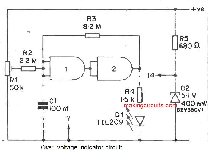
If the supply voltage goes above a predetermined level, the voltage at the input of the trigger circuit will surpass the upper threshold voltage, and the output of the circuit will go high. Current will then be delivered to D1 that may, in consequence, can occur and reveal the excessive supply voltage.
The circuit can be adjusted to work at any voltage from about 3 to 15 volts. In an effort to provide R1 the correct setting it is essential to connect the unit to a supply voltage which is equal to the desired threshold voltage. R1 is then adjusted for the lowest slider voltage which in turn causes D1 to come on.
Due to the fact that the circuit has a degree of hysteresis, it is important to begin with R1 slider at minimum voltage, and then slowly increase this till D1 illuminates. Beginning with R1 slider at maximum voltage and then turning it back prior to the L.E.D. fades is simply not right.
If this is carried out, the lower theshold voltage of the Schmitt trigger will probably be attained when the input voltage reaches the overload point, although it ought to be the upper threshold voltage that is achieved. The circuit might then fail to interact to a somewhat substantial voltage.