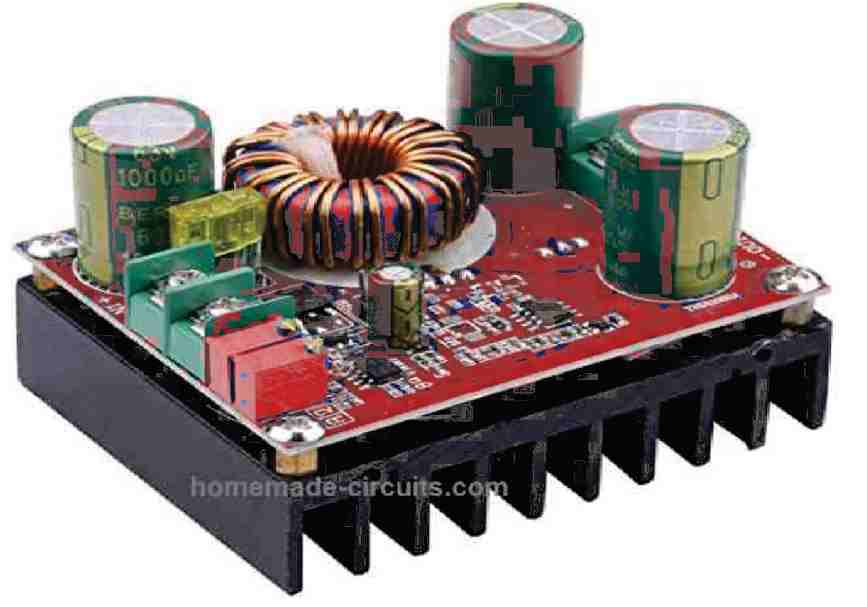
A basic circuit for a 12 V to 19 V boost converter that can be utilized for charging a 19 V battery from a 12 V automobile battery is described in the post that follows.
The primary use of this circuit may be to charge a laptop battery using a vehicle battery.
Circuit Overview
We present a diagram of the circuit that converts 12 V to 19 V.
Circuit Operation
The operation of this circuit is simple.
We use a free running astable oscillator to generate a square wave signal. This signal drives a voltage doubler circuit which boosts the voltage from 12 V.
To keep the output voltage stable we include a series pass transistor. This transistor works like a variable resistor which adjusts its resistance based on the output voltage needs. A comparator monitors the output voltage and gives feedback to the transistor which helps it to regulate the voltage.
Ground Connections
We connect the ground for both the input and output lines to the negative terminal of the 12 V power source. This common ground is essential for the circuits proper functioning which ensures that all voltage measurements are accurate.
In our astable multivibrator setup we use IC1B as the main active part. We place capacitor C1 and resistor R4 in the feedback path to create a frequency around 15 kHz.
To keep the square wave output at a balanced 50:50 duty cycle, we need diode D1 and resistor R7 to work properly.
We must choose a high-quality capacitor C1. It should have good stability and a low temperature coefficient. A ceramic capacitor is usually a good choice.
Diode D1 also needs to have temperature characteristics that help maintain the output square wave regardless of load changes and heat in the circuit.
Transistors T2 and T3 turn on alternately with the square waves from IC1B.
When T3 is ON capacitor C3 charges to 12 V through diode D2. Then when T3 turns OFF, T2 activates and connects the negative side of C3 to the +12 V supply.
In this case the charge in C3 cannot change instantly. So when we connect the negative terminal to 12 V, the positive terminal must also rise. This makes the positive terminal of C3 reach about double the supply voltage.
However due to losses in diodes and transistors, we will not get exactly twice the supply voltage. The output will be slightly less than expected.
To fix this we use Schottky diodes to reduce the forward voltage drop. Diode D3 rectifies the voltage while capacitor C4 stores this rectified output.
We must select a very high-quality capacitor for C3 since it provides all the output current to the load. We manage the output voltage with op-amp IC1A.
We have resistors R14 and R12 arranged as a potential divider. This setup helps us to sense the voltage at the collector of T4. Then IC1A compares this sensed voltage to a reference voltage created by R6, R9, and the zener diode D4.
To get a stable output voltage of 19 V we can change the resistance of R14. If we set R14 to 15 kΩ then output voltage will be about 19 V.
The ripple voltage in the 19 V output under full load will be shown in the next figure.
When power is initially turned on, increasing the quantity of capacitor C6 will guarantee that the reference voltage increases extremely slowly. This function may offer the circuit for the 12 V to 19 V converter a pleasant slow-start or soft-start feature. The LED D6 could be used to confirm this switch-on delay.
Design of PCBs
The following graphic displays the components overlay diagram and the entire PCB design:
