

The post details how to build a simple 30 watt stereo power amplifier circuit using a single hassle free IC TDA1521
This little (yet strong) stereo very compact could be effortlessly repaired and troubleshot.
This Philips monolithic integrated circuit TDA1521, that contains an ultimate dual BF with totally self-employed channels, each competent at delivering 10 to 12 W To an 8 ohm or 15 W on 4 ohm (30 W musical) speaker. The gain from the amplifiers is placed at 30 dB (around 32 times). And all this
Using just a couple of compensating networks in parallel on the outputs and a couple of capacitors to decouple the inputs! That is almost all. This high degree of incorporation assists you to be happy with a printed circuit of 5 x 7 cm which includes in addition the rectifier bridge and the capacitors of smoothing of the power supply.
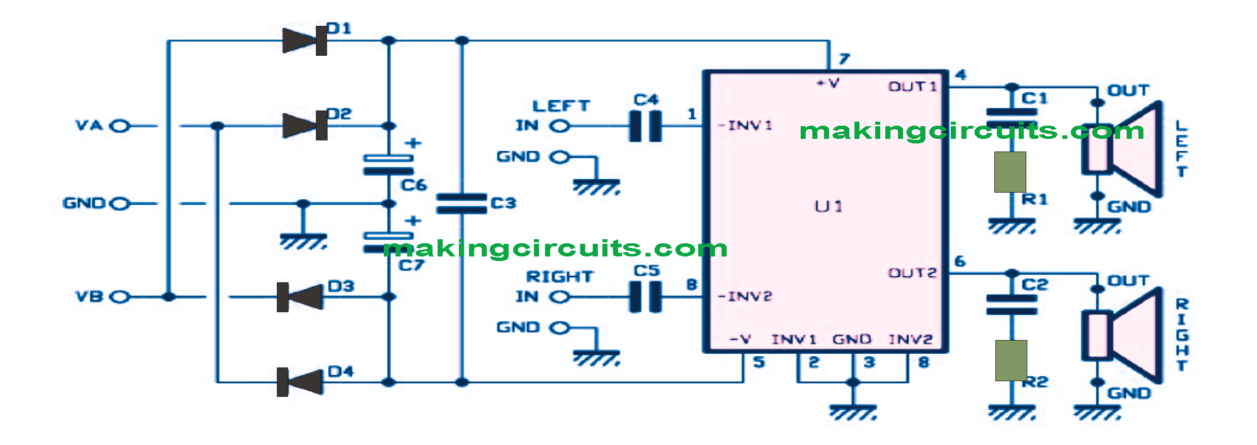
The electrical diagram of FIG. 1 displays the level that this integrated circuit can make it easy to create a Hi-Fi amplifier working having a symmetrical double feed: we are going to examine only one of the two channels (another being identical ) Pointed out INV1, -INV1 and OUT1. All of us prefer
The settings offering for the application of the signal to the input -INV (non-inverting) based on the ground. Because the power supply is dual, we are able to ground the inverting inputs (INV1 and INV2, respectively pins 2 and 8) and the reference point (pin 3). Therefore, the feedback system is definitely a parallel / series since it requires a part of the output voltage and exchanges it to the inverting input of the first operational amplifier with the bridge created of resistors of 20 k and 680 k. The input signal of the circuit extends to pin 1 via C4, it is amplified for the first time and, at the output of a 1st amp-op stage, goes by to the input of a second one that boosts the level And reverses its Phase prior to delivering it to the power segment produced in contributory balance by two built-in transistors, an NPN and a PNP. These BJTs run in emitter-follower, so that they merely amplify in current and leave one other phase signal as it was at the input of the circuit
integrated. First conclusion: Inverting (INV) and non-inverting (-INV) make reference to the inputs of the first operational amplifier and never to the entire amplifier. Without a doubt, to possess a signal
Output in phase using the one sent to the integrated circuit, it should be shipped to the inverter (by shutting to the ground -INV) in contrast to when it is provided for the non-inverting and INV to GND, as in Our own program, the entire amplifier gets, actually, inverter. In functioning with a sinusoidal input wave at 1 kHz, achieving the loudspeaker is actually a voltage of the same envelope and frequency, with an amplitude
Around 32 times higher but out of phase by 180 °.
The TDA1521 features a number of protections, in addition to a delay network that, in the transient of
Switches off the input stage to prevent amplifying the LF prior to the power supply has attained its speed values: in parallel using the input, there exists a second op-amp, The last mentioned should never amplify anything but give a reference voltage to the subsequent stage throughout power-up. A voltage window comparator comprising two op amps regarded as "Voltage Comparator"
Monitors the power supply. In function, the two resistors of 10 k figure out precisely 0 V on the line terminating at pin 3, ie the ground potential. "In operation" ... but while the power is switched on it is extremely probable that asymmetries take place
And that the potential on the positive series is different considerably from that of the negative. Because the signal BF could be delivered very distorted, it really is worthless to amplify it therefore, the comparator, sensing the abnormality, places the outputs of the two op amps in the low level (0 V) and intervenes on the "Switch" CMOS that delivers the supply voltage of the preamplifier stages towards the points Vr, by deactivating the first op amps and making just those of reference to operate. This ensues that the a couple of, attached to Vref1, polarize the inverting "inputs" of the 2nd stages with
This potential (Vref1, exactly ...) simply to maintain the whole amplifiers in balance. When the power is nicely balanced, the window comparator updates it, sets its output level high and regulates the CMOS "switch" to drive the voltage Vp to the input ampli-op, ie those given by The line Vb. The reference polarization is then turned off and the music signal could be amplified and brought to the speakers.
Regarding these, the TDA1521 offers short circuit protection on output terminals (on a single or each channels) ... for just one hour! Protection can also be induced in the event of overload, ie if the load impedance is too low and demands more current than the highest permissible.
We will now leave the integrated circuit to obtain the existence of C4 and C8, essential for the decoupling of the inputs and the R / C dipoles, each and every in parallel with one of the loudspeakers (or loudspeakers): these RC networks in order to partly make up the rotation. C1 and C2 make up for the phase shift that the loudspeakers,
Through their inductive nature, bring in between voltage and current: the objective of this compensation is to steer clear of the phase shift becoming adequately noticeable to convey, via the feedback, a LF component able to generating a self-oscillation of the amplifier as a whole.
When it comes to power supply, that is partially on the circuit board (not the transformer!), It has 3 input points VA, GND, VB, that obtain the three outputs of the symmetrical center-tap secondary. D1, D2, D3, D4 form a rectifier bridge that makes it feasible to rectify the AC voltage supplied by the transformer in positive half-wave the current of the upper winding Navigate D2 and load C6 with a sinusoidal instinct after which come back by the ground to the central socket. The low winding offers a current to C7 with the center tap that returns through the negative via D3. Within negative half-wave D3 and D2 tend to be forbidden while D1 and D4 carry out: the current
Moves via VB via D1 to C6 that charges with a brand new sinusoidal pulse, simultaneously one more pulse of equal amplitude goes by with the mass, load C7 and comes back through
D4 on VA. As a result of the particular settings of the bridge diodes, electrolytic
Are subjected to current pulses at the frequency of 100 Hz (2 for every time period) which charge these to compensate for the energy they produce to the TD1521 in regular usage. C3 filters any disturbances from the transformer. The whole circuit calls for a double 12 + 12 Vfc alternating voltage, which takes in a bit more than 16 Vdc on each branch (+16 Vdc between pin 7 of the integrated circuit and the mass, -16 Vdc between pin 5 and GND) Uses 70 mA at rest (in the lack of signal
Input) and 2 A at highest power on 4-ohm speakers.
Diagram showing the components of the stereo amplifier.
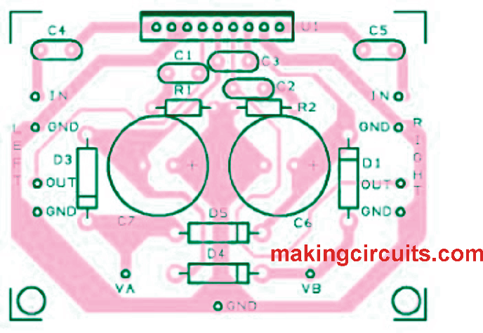

Drawing the stereo amplifier printed circuit board to scale 1.


The practical implementation
The practical acknowledgement of this Hi-Fi stereo amplifier could barely be less complicated: indeed the simple printed circuit offers just a few elements and the solitary integrated circuit SIL obviously does not have any support! Figure 2b shows the style of the small printed circuit board at level 1. If you have it in front of you, attach the several components besides the integrated circuit, finishing with the a couple of large electrolytic capacitors.
Additionally, screw the integrated circuit on the heatsink (this should have an Rth of 3.3 ° C / W maximum) using the a couple of bolts, keeping in mind to put a sheet of mica or teflon insulation and a couple of Slim and regular layers of white silicone thermal paste known as "compound" to both the sides of the insulation piece. After that, twine its tabs into the gaps of the printed circuit board and weld all of them, after that slice extra lengths.
If you wish to install your amplifier within a case, try some fine metallic model.
Application tests:
Hook up a pair of speakers with impedance no less than 4 ohms, switch on (2 x 9 to 15 Vac), after which attach a stereo sound source to the input. This particular should be built with a level control program, or else precede each channel having a potentiometer
Whose slider or knb shall be linked to capacitor C4 or C5 of 1 μF, one end to ground as well as the other to the inbound LF source (utilizing a dual potentiometer is more preferable). See figure 4.
List of components:
R1 = 8.2 Ω 1/4 W
R2 = 8.2 Ω 1/4 W
C1 =22 nF ceramic
C2 = 22 nF ceramic
C3 = 100 nF multilayer
C4, C5 = 1 μF 63 V polyester
C6 = 4 700 μF 25 V
electrolytic
C7 = 4 700 μF 25 V
electrolytic
D1----D4 = 1N5404
U1 .... TDA1521
Misc:
1 ...... heatsink
(Rth less than 3.3 ° C / W)
2 ...... bolts 3MA 12 mm
Unless otherwise specified, all
Resistors are 1/4 W at 5%.
TECHNICAL CHARACTERISTICS
- Power supply: balanced 12 V balanced voltage
- Maximum output power RMS:
2 x 15 W / 4 ohms, 2 x 10 W / 8 ohms
- Maximum musical output power:
2 x 30 W / 4 ohms
- Harmonic Distortion: 0.007% (1 W / 1 kHz)
- Input sensitivity: 300 mV / 20 kilohms
- Frequency: from 7 Hz to 60 kHz (-3 dB)
- 70 dB for each channel
- Output power (R1 = 8 ohms):
2 x 10 W RMS
- Output power (R1 = 4 ohms):
2 x 15 W RMS
- Bandwidth (-3 dB): 7 to 60,000 Hz
- Sensitivity to maximum power (8 ohms):
290 mVeff
- Sensitivity to maximum power (4 ohms):
250 mVeff
- Input impedance: 20 kilohms
- Signal-to-noise ratio: 98 dB
- Crosstalk: -70 dB
- Excellent stereo amplification
- Low noise
- Overload protection:
Maximum one hour.