

In this post we learn how to build simple amplifier circuits using digital CMOS ICs, such as a NAND gate IC 4001
With regard to non -critical amplifier applications, and as the basis of various kinds of oscillator, CMOS I.C.s certainly are a very eye-catching proposal as a result of ease-of-use of the circuitry and their cost effective.
Simple Amplifier
The circuit diagram of a very easy CMOS amplifier which usually works with a single inverter is demonstrated in Figure below. R1 is utilized to bias the inverter as a linear amplifier. The output of the device will start to go high when the supply is at first connected, considering that the input will be low.

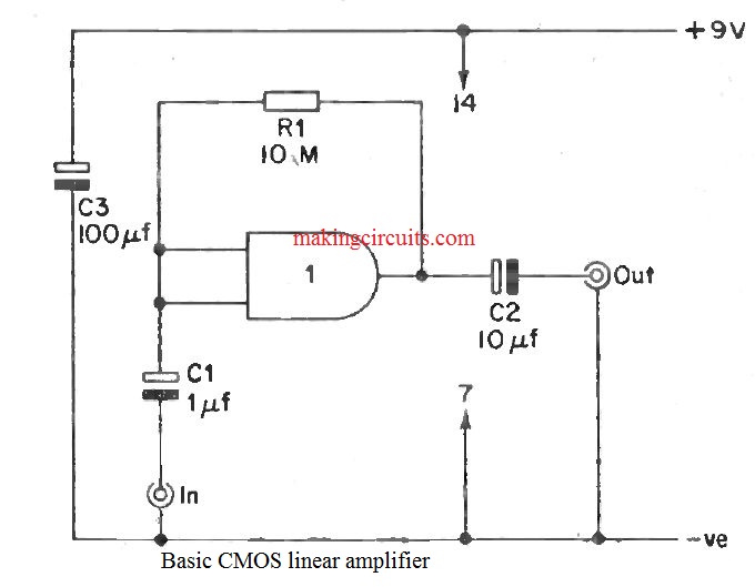
Once the voltage at the output extends to the transfer voltage of the gate, the input will attempt to consider the output low as the input will probably be taken high by the voltage acquired by way of R1 from the output. The output voltage will probably be stabilised at around half the supply potential by this negative comments activity. The gate is therefore biased into a linear mode.
At sound frequencies this particular circuit provides a voltage gain of around 50 times, as well as at a frequency of numerous MHz it will eventually continue to supply a degree of gain. It is not designed for use within Hi-Fi circuits, and is actually best suited for non -critical applications, for example in the peak level indicator which has been explained previously.
The significance of R1 is not really crucial, however it must be in the Megohm region if the full voltage gain of the circuit is to be noticed. C1 and C2 are the input and output D.C. obstructing capacitors respectively. It isn't a smart idea to make use of this circuit with a nominal supply voltage of lower than around 9 V as it could possibly then turn out to be unstable.
Operational Amplifier
A far more advanced amplifier could be generated by cascading three inverters collectively, as demonstrated in below diagram. This circuit is biased into a linear functioning situation by R2, which usually functions in very similar method as R1 from diagram Basic CMOS linear amplifier.

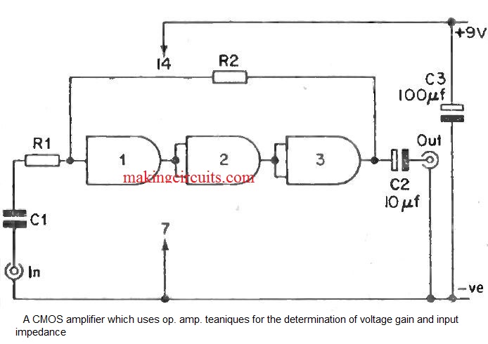
Functional amplifier methods are accustomed to choose the preferred input impedance and voltage gain of the circuit, and this creates the circuit very convenient without a doubt. The input impedance of the circuit is equal to the value directed at R1, and the value of R2 is calculated by multiplying that of R1 by the needed voltage gain
Input impedances in the Megohm region are often achieved, as are very high voltage gains, however it is not actually realistic to acquire these two in the similar amplifier. There is the issue that the essential high value resistor for R2 would merely not be accessible, and stability would possibly be dropped even though an appropriate component was utilised.
The circuit has an open loop gain of typically 125,000 times (50 x 50 x 50 = 125,000), and a significant amount of negative suggestions is therefore placed on the circuit when it is employed in a practical conditions with a closed loop gain of possibly only 10 or 20.
This allows the circuit with a sensible level of effectiveness pertaining to noise and distortion, but it is not meant for high quality sound use. You ought to make use of a effective component layout which can be free from extreme stay capacitances, particularly when the circuit has been employed having an input impedance of more than a couple of k. Or else there is a possibility of the circuit turning into unstable.