Transistors can be understood as an active semiconductor device having 3 pins or terminals, designed to either block or allow a bigger current in response to a smaller current.
This feature of transistors to switch from an ON state to an OFF state allows to work effectively as solid-sate or digital switches and also as current amplifiers (analogue current boosters).
More precisely transistors are built to operate across the following three regions:
Active Region: Where the transistor work like current amplifier having Ic = ßxIb
Saturation: Where the transistor is enabled to be Fully Switched ON, and functioning like a digital switch, having Ic = I(saturation)
Cut off: Converse of the switch ON, here the transistor is working a switched OFF switch, having Ic = 0
Transistors are designed with two fundamental internal structures, namely PNP and NPN, which tells us how their internal structure are constructed using P-type and N-type semiconductor materials.
Let's consider a BJT or a Bipolar Junction Transistor internal structure, which has a couple of PN-junctions creating 3 linked terminals attributed with 3 unique names for identifying one from the other, which are as follows:
These terminals also called called transistor pinouts are designated as:
Emitter (E), Base (B), and Collector (C), in an order depending on how the device is positioned.
BJTs are basically current controllers or regulators, wherein the amount of current conduction across their collector emitter pins depends on the proportion of small biasing current passing across their base and emitter pins. This enables them to work like a current regulating switches or devices, since we are able to manipulate a small amount of current across base emitter terminals to control the flow of a relatively large amount of current across the collector emitter terminals.
The working principle of both the variants PNP or NPN are identical, except their biasing polarity and the polarity of the supply rails associated with a given configuration.
A Typical Bipolar Transistor


Bipolar Transistor Construction
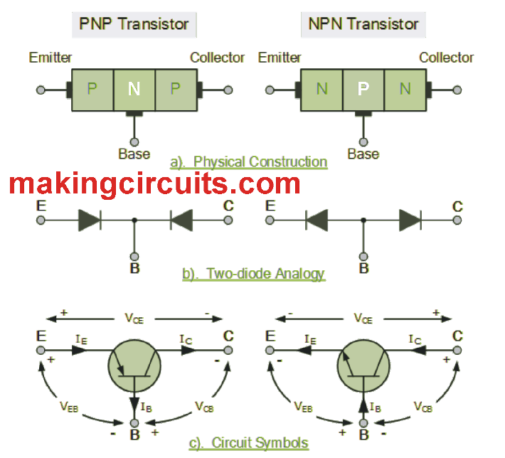
We can see the symbols of PNP and NPN transistors as used in electronic circuits.

The arrow head of the particular terminal basically indicates the exit direction of conventional current flow, across the base emitter terminals of the device.
The arrow direction always represents the flow of current from the positive P-type region towards the negative N-type region for both the variants PNP and NPN, precisely as we find in rectifier diode symbol.
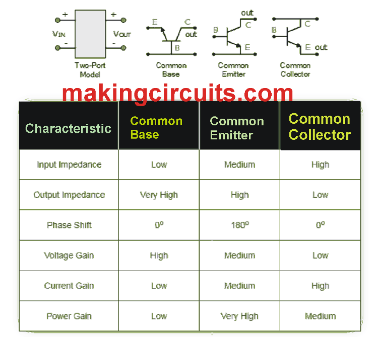
Bipolar Transistor Configurations
With 3 terminals assigned to a BJT or a bipolar transistor, it becomes possible for us to configure these devices in 3 unique ways in a circuit depending on the application requirement. In each of these configurations we have one input option, one output option, where the emitter acts like a common terminals for both the options.
Common Base Configuration – shows Voltage Gain without any Current Gain.
Common Emitter Configuration – shows both Current and Voltage Gain.
Common Collector Configuration – shows Current Gain but no Voltage Gain.
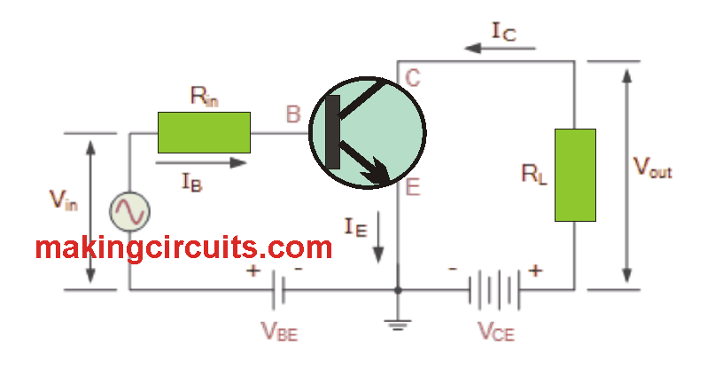
The Common Base (CB) Configuration
The input signal is fed across the base and emitter of the BJT, and the resulting output signal is derived across the base and the collector terminals of the BJT. The base signal is always referenced to the emitter terminal and its potential level.
The Common Base Transistor Circuit


A common base BJT circuit behaves like a non-inverting amplifier circuit, due to the fact that its output signals is always in-phase with the input signal, meaning the output precisely replicates the input signal's polarity without changing its attributes.
This configuration is normally avoided since it creates a rather high voltage gain characteristics, wherein the input characteristic can be compared to a forward biased diode and the output characteristics to an illuminated LED.
Additionally this kind of bipolar transistor arrangement features a high ratio of output to input resistance or more notably “load” resistance ( RL ) to “input” resistance ( Rin ) presenting it a value of “Resistance Gain”. As a result the voltage gain ( Av ) for a common base configuration is presented as:
Common Base Voltage Gain
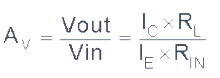

In which: Ic/Ie is the current gain, alpha ( a ) and RL/Rin is the resistance gain.
The common base circuit is commonly exclusively used in single stage amplifier circuits for instance microphone pre-amplifier or radio frequency ( Rƒ ) amplifiers because of its excellent high frequency processing.
The Common Emitter (CE) Configuration
In the Common Emitter or grounded emitter configuration, the input signal is placed across the base and the emitter, while the output is extracted from across the collector and the emitter as demonstrated. This sort of arrangement is one of the widely used circuit for transistor based amplifiers and it signifies the “normal” approach to bipolar transistor network.
The common emitter amplifier construction delivers the very best current and power gain among the 3 bipolar transistor designs. This is largely because the input impedance is SMALL since it is attached to a forward biased PN-junction, while the output impedance is LARGE since it is obtained from a reverse biased PN-junction.
The Common Emitter Amplifier Circuit

In this form of configuration, the current moving from the transistor needs to be the same to the currents coming in into the transistor in the form of emitter current can be presented as Ie = Ic + Ib.
Since the load resistance ( RL ) is joined in series with the collector, for a common emitter transistor configuration the current gain can be pretty large simply because it is the ratio of Ic/Ib. A transistors current gain is represented through the Greek symbol Beta, ( ß ).
Because the emitter current for a common emitter configuration is characterized by Ie = Ic + Ib, the ratio of Ic/Ie is known as Alpha, symbolized by the Greek symbol of a. Take note: that the value of Alpha will at all times be lower than unity.
Considering that the electrical relationship between these 3 currents, Ib, Ic and Ie depends upon the physical structure of the transistor alone, a slightest of variation in the base current ( Ib ), may lead to a significantly larger improvement in the collector current ( Ic ).
Subsequently, little changes in current moving within the base may as a result regulate the current across the emitter-collector circuit.
Simply by merging the expressions for both Alpha, a and Beta, ß the numerical relationship between these variables and consequently the current gain of the transistor could be expressed as:


Where: “Ic” is the current moving towards the collector terminal, “Ib” is the current going towards the base terminal and “Ie” is the current flowing out from the emitter terminal.
Therefore to sum up the whole thing. This sort of bipolar transistor configuration includes a higher input impedance, current and power gain compared to that of the common base configuration nevertheless voltage gain can be a lot lower. The common emitter configuration is an inverting amplifier circuit. Meaning, the ensuing output signal carries a 180 degree phase-shift in relation to input voltage signal.
The Common Collector (CC) Configuration
In the Common Collector or grounded collector configuration, the collector now becomes common reference with regards to the supply. The input signal is hooked up straight to the base, whereas the output is extracted through the emitter load as indicated in the diagram. This kind of arrangement is usually recognized as a Voltage Follower or Emitter Follower circuit.
The common collector, or emitter follower construction is incredibly helpful for impedance matching applications due to its extremely high input impedance, approximately thousands of Ohms while featuring a comparatively lower output impedance.
The Common Collector Transistor Circuit


The common emitter arrangement features a current gain roughly equivalent to the ß value of the transistor itself.
Since the emitter current is the combined result of the collector AND the base current put together,
The Common Collector Current Gain


This kind of bipolar transistor configuration is a non-inverting circuit wherein the voltages Vin and Vout tend to be “in-phase”. It carries a voltage gain which is at all times lower than “1” (unity).
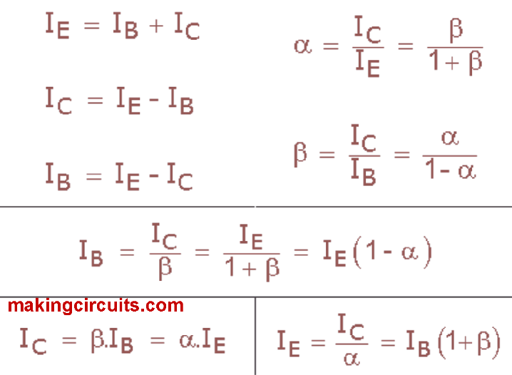
We can at this point review the different relationships between the specific transistor DC currents flowing via each terminal and its DC current gains discussed above, within the following table.
Relationship between DC Currents and Gains

Bipolar Transistor Summary
To sum up, the working nature of bipolar transistors in each one of the above circuit designs can be quite diverse and delivers distinct circuit characteristics in terms of input impedance, output impedance and gain, which may be voltage gain, current gain or power gain and all these are described in the table listed below through the general attributes of the various transistor configurations:.
Bipolar Transistor Configurations