


The following simple yet, improved, TL494 zero drop buck solar battery charger circuit works extremely well together with almost any solar panel intended for charging cellphones or cell phone battery packs in numerous quantities rapidly, simply the circuit has the ability to with charging any battery whether or not Li-ion or Lead acid that could be around the 5V range.
The style is founded on a SMPS buck converter topology utilizing the IC TL 494 (I have turn into a huge fan with this IC). Owing to "Texas Instruments" for delivering fantastic IC to all of us.

We understand that a 5V solar charger circuit may be effortlessly designed implementing linear ICs such as LM 317 or LM 338,
Despite this the largest downside with such linear chargers could be the release of heat by means of their body or by way of package dissipation, resulting in wastage of valuable energy. For this reason or issue these kinds of IC aren't able to make a zero drop voltage output for any load and demand at the very least 3V increased inputs compared to the particular outputs.
The circuit of the 5V charger discussed at this point is totally free from all of these headaches, let's discover how an effective functioning can be accomplished through the offered circuit.
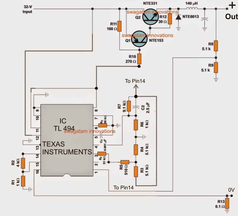
With reference to the above mentioned 5V PWM solar charger circuit, the IC TL494 constitutes the center of the whole program.
The IC is actually a professional PULSE WIDTH MODULATION processor chip IC, utilized in charge of maintaining a buck converter stage, accountable for switching the high input voltage into a recommended reduced output.
The input towards the circuit could be ranging from 10 and 40V, which usually turns into the best assortment for your solar panels.
The crucial element of the IC consists of:
Accurate PWM output which can be adaptable depending on consumer requirements.
To be able to produce genuine PWMs, the IC incorporates a highly accurate 5V reference created by applying bandgap principle making it thermally resistant. This specific 5V reference which can be attained in pin#14 of the IC gets to be the base voltage for all the essential invokes included around the IC and in control of the PWM control.
The IC includes a couple of outputs which is often possibly put together to oscillate in tandem within a totem pole construction, or perhaps equally at any given time similar to a single ended oscillatory output. The very first alternative results in being well suited for push-pull type of programs for example in inverters etc.
Except for the current plan just one ended oscillatory output results in being better and also this is accomplished through grounding pin#13 of the IC, additionally with regard to obtaining a push pull output pin#13 could possibly be attached with pin#14,
The outputs of the IC features a very beneficial and an appealing assemblage inside. The outputs tend to be ended through a couple of transistors within the IC. These types of transistors are usually put in place using an open emitter/collector throughout the pin9/10 and pins 8/11 correspondingly.
Regarding purposes that call for a positive output, the emitters works extremely well as the outputs, that exist through pins9/10. With regard to this kind of programs typically an NPN BJT or an Nmosfet could well be put together outwardly for agreeing to the positive frequency throughout the pin9/10 of the IC.
In the current layout because a PNP is utilized together with the IC outputs, a negative sinking voltage gets to be the best choice, and for that reason as opposed to pin9/10, we now have associated pin8/11 with all the output stage including the PNP/NPN crossbreed stage. These outputs present adequate sinking current intended for running the output stage as well as for operating the high current buck converter arrangement.
PWM Buck Control
The PWM rendering, which usually gets to be the key element for any circuit is accomplished by serving a sample feed-back transmission to the interior error amplifier of the IC by means of its non-inverting input pin#1.
This PWM input are seen installed using the output in the buck converter by way of the potential divider R8/R9, and also this feedback cycle inputs the mandatory information for the IC in order that the IC has the capacity to produce manipulated PWMs throughout the outputs so that the output voltage persistently stays at 5V.
Additional output voltage could be predetermined by merely modifying the valuations of R8/R9 according to ones personal program demands.
Charging Current Control
The IC possesses a couple of error amplifiers established in house intended for governing the PWM according to outside feedback impulses. One of many error amp is employed for governing the 5V outputs as talked about previously, the next error amp is needed for manipulating the output current.
R13 becomes the current sensing resistor, the potential produced throughout it is actually raised on to one of inputs pin#16 of the subsequent error amp which can be investigated with the reference at pin#15 put on the opposite input of the opamp.
Within the suggested layout it can be established for 10amp by way of R1/R2, which means in the event the output current will probably boost above 10amps, the pin16 should be expected to go beyond the reference point pin15 starting the specified PWM compression till the current is fixed back to the desired ranges.
Buck Power Converter
The power level demonstrated in the layout is really a regular power buck converter stage, employing a hybrid Darlington pair transistors NTE153/NTE331.
This hybrid Darlington stage takes action with the PWM manipulated frequency from pin8/11 of the IC and runs the buck converter stage which involves a high current inductor along with a high-speed switching diode NTE6013.
The above mentioned level creates a highly accurate 5v output guaranteeing minimal turbulence along with a prefect zero drop output.
The coil or the inductor could be wound around virtually any ferrite core having a 3 simultaneous strands of super enameled copper wire each and every using a dimension of 1mm, the inductance value could be just about anywhere around 140uH for the recommended layout.
Hence this particular TL494 based buck battery charger circuit can be viewed as a possible perfect and incredibly effective solar charger circuit for many kinds of solar battery charging programs.