


The submit clearly shows a cell phone remote control circuit implementing the light from its display.
The suggested cell phone display light remote control circuit could possibly be observed in the presented diagram. The information might be known from the following clarification:
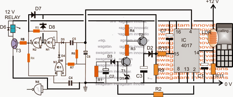
The circuit fundamentally includes three phases: the left flip flop stage utilizing NAND gates, the center delay ON stage applying BJTs T1, T2 and the right side is a light detector and processor circuit stage implementing the IC 4017.
When power is first switched, the capacitor attached across pin15/positive of IC 4017 resets the IC making certain that at begin pin 4 and pin 2 of the IC generates logic zero.
Presuming the cell phone display to be inactive, the LDR is kept at complete darkness being sure an entirely neutral and a deactivated situation of the circuit.
Right now guess a call is made on the linked cell phone, it's display lights up producing a low resistance on the LDR which often permits a confident "clock" to strike pin14 of the IC 4017.
This causes the IC to move its logic high from its pin3 to pin2. At this position the cell phone display light duration or the call duration become irrelevant could be disregarded.
Nevertheless the high at pin2 starts charging C2 via R2 to be able to switch on the delay ON timer comprised of T1 and T2.
Believe absolutely no additional call is created on the cell phone in this required and the display is permitted to close off, pin2 goes on charging C2 until the potential stage at the base of T1 goes up to a point of saturation turning on T1 and T2. T2 collector immediately directs a positive signal at pin15 of IC 4017 forcing it to reset getting rid of the pin2 high across C2 and restoring the IC to its earlier standby position.
In spite of this, believe while C2 was charging and before T1 can perform an additional call was designed on the cell phone, might have produced another "clock" at pin14 of the IC4017, making its output to shift from pin2 to pin4.
In the above circumstance eliminating pin2 high stops the delay ON timer from signaling and its role is taken away in this circumstance but the high shift at pin4 transmits a positive pulse to the flip flop stage, leading to the relay to alter state either from N/C to N/O or vice versa based upon its first scenario.
The moment the flip flop gets involved itself and the relay into a flipped mode, a positive from the relevant output of either N1 or N2 is given back to pin15 of IC 4017 resetting it back to its original standby position for the next activating cycle.
Consequently the relay becomes effectively started or deactivated for toggling the associated load ON/OFF with the above methods.
All following couple of calls made on the modem cell phone within the stipulated time brings about the relay ON and OFF which inturn is utilized for toggling any appropriate load across the contacts.
The unit might be regarded as completely quick and easy as a result of the incorporation of a timed and paired signal inputs from the cell phone.
Parts List
R1, R7, R6, R11 = 100K
R2 = 330K
R3, R4, R10, R8 = 10K
R5, R5, R9 = 2M2
T1, T3 = BC547
T3 = BC557
D1 = 3V ZENER
D2---D8 = 1N4148
C1,C3 = 1uF/25V
C2 = 1000uF/25V
C4, C5 = 0.22uF
C6, C7 = 10uF/25V
N1----N4 = IC 4093
LDR = SHOULD BE AROUND 10K TO 33K IN CELL PHONE LIGHT
