

The post details many interesting and easy to build FET and MOSFET circuits, which can be used in everyday life in many useful applications.
The IRF511 N-channel power MOSFET is easily one of the cheapest hexFET components. It has a maximum on-state resistance of 0.6 Ω, input/output capacitance of less than 150 picofarads (pF), a gate-controlling voltage of between 2 and 4 V, a maximum drain-to-source voltage of 60 V and a maximum drain current of 3 A.
Further, the device occupies maximum power dissipation of 20 Watts and is compactly packaged.
The variety of application circuits this semiconductor FET device can be applied includes inverters, choppers, switching power-supplies, motor speed controls, audio boosters and high-energy pulse circuits.
Class A Amplifier


The first Figure above displays the IRF511 in a class-A audio amplifier circuit. When zero gate bias is applied, Q1 acts as if it is in the off state, therefore no current flow is present via the load resistor R2.
The voltage across Q1 and the load resistor should be the same for class-A operation.
A 100k potentiometer (R3) and a 1 MΩ fixed resistor (R1) forms a standard adjustable gate-bias circuit.
Use a voltmeter between Q1’s drain and the circuit ground and regulate R3. You will see the meter reads 50% of the supplied power.
You can opt for any value for R2 as long as the maximum current and power ratings of the FET are not crossed.
We advise to choose any value between 22 and 100 Ω when you’re testing this circuit. It is good to remember to incorporate a heat sink when using high currents.
Relay Controller

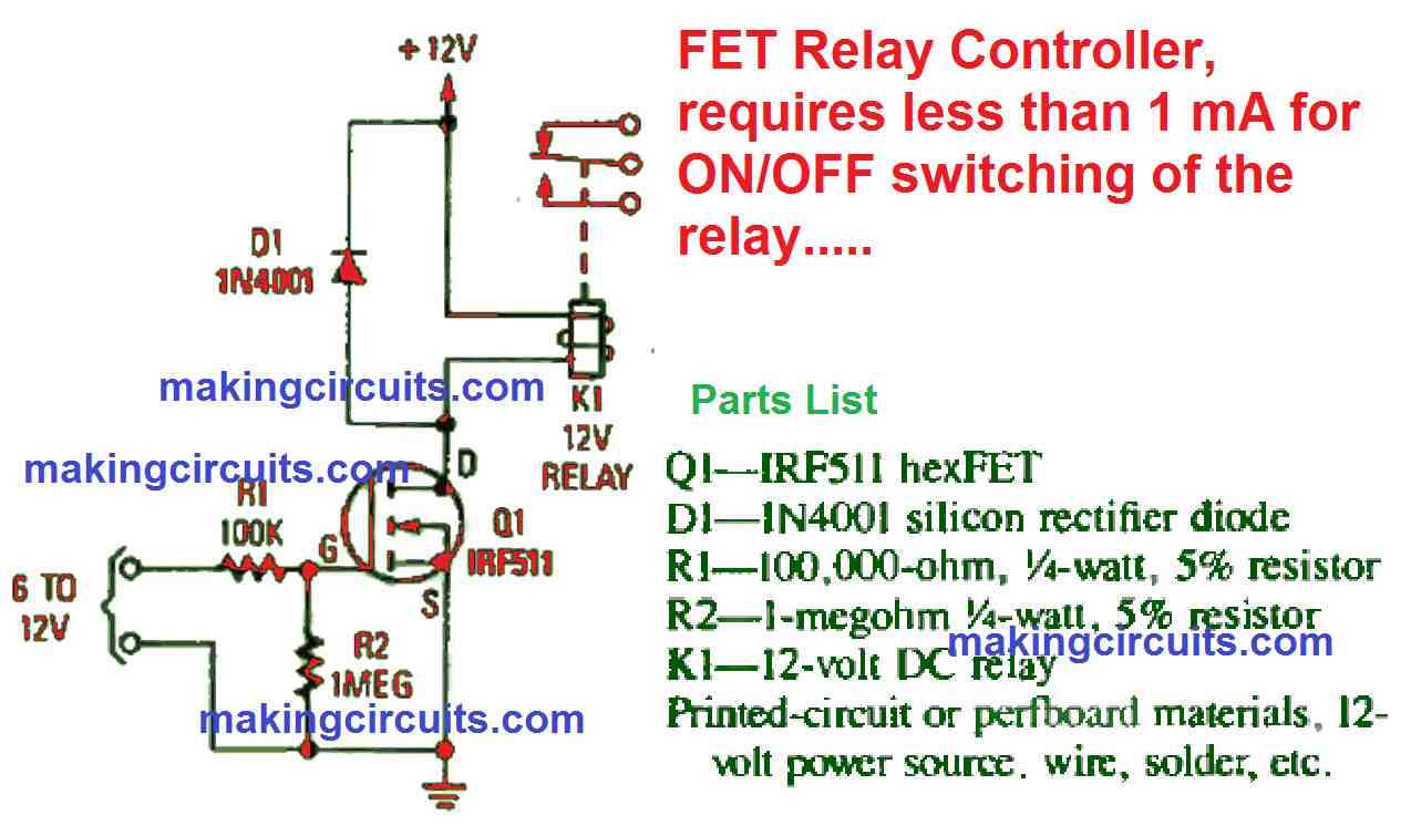
Another circuit as depicted in Figure above has the power FET (Q1) governing a relay. Q1 functions like an open-switch when zero gate-bias is applied.
However, if a DC voltage of more than 5 V is supplied to the circuit’s input sections, Q1 will be on. This action closes the connection of the relay circuit leading to activation of the relay coil.
You will just need less than 10 µA of input bias current to trigger Q1 and operate the relay.
The required current is 1 million times smaller than what is required to bias the famous 2N3055 power transistor to work the same relay.
Proximity Switch

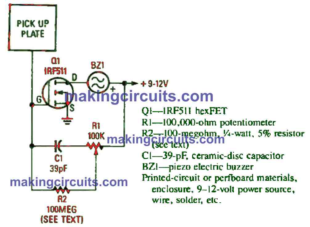
In our next circuit as presented above, we will discuss the extremely high input impedance and the power-regulation capabilities of the FET to construct a standard yet sensitive proximity sensor and an alarm-driver circuit.
You can use a 3 x 3-inch circuit board or any relevant metal piece that can operate as a pick-up sensor. This must be connected to the gate of Q1.
Use a 100 MΩ resistor as R2 which isolates the Q1’s gate from R1. This action permits the input impedance to stay exceedingly high.
If a 100 MΩ is unavailable, you can connect five 22-MΩ resistors in series and apply that as R2. It is good to know that to increase the sensitivity just increase the R2 value.
Potentiometer R1 is tuned to a point where the piezo buzzer just starts to click off. Immediately back off slightly to a point where the buzzer stops making noise.
Testing the setting of R1 will assist in getting the best sensitivity adjustment for the circuit. You can also set resistor R1 to a point where the pick-up must be linked to trigger the alarm.
As an alternative to the piezo sounder, you may use a relay or other current-chasing component to govern any external circuit.
Lamp Flasher
The circuit as shown below is constructed around two power FETs, which are set as typical astable multivibrator to interchangeably turn the pair of lamps on and off. The R/C values displayed in the Parts List sets the flash rate around 0.333 Hz.


By changing one of the resistor or capacitor values, you can get almost any flash rate. Rise the values of either C1 and C2, or R1 and R2 to delay the flash rate. To boost the rates, just decrease the R/C components values.
The power MOSFETS aren’t like any other semiconductor devices because they can be paralleled without needing current-sharing devices which are required to regulate bigger load currents.
This is crucial when such devices are utilized to switch on incandescent lamps due to the lamp’s cold resistance. Generally, cold resistance is lesser than normal operating resistance.
Using a standard #18151 12- to 14-V lamp which measures around 6 Ω is supplied with 12 V, the initial current drawn is close to 2 A. With the same lamp, when you operate at 12 V, it only needs 200 mA.
In this case, the hot resistance is known to be at least 10 times its cold resistance, or 60 Ω. This is knowledge is vital when choosing any semiconductor component to control an incandescent lamp.
Variable Frequency (VFO) Oscillator

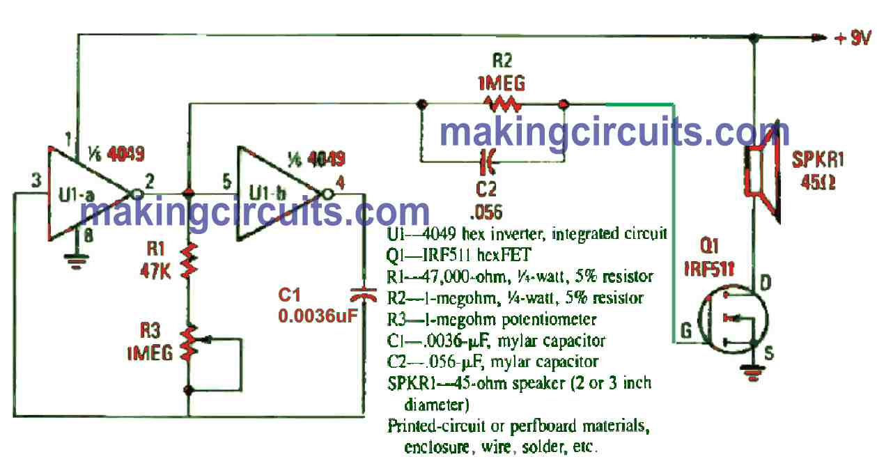
Next, we look into the diagram above that has the power FET in the output stage of an audio variable frequency oscillator (VFO) circuit.
This FET VFO circuit can be deployed to examine audible-tone testing and be transformed into a typical electronic musical instrument.
For example, a handful of them can be wired parallel to each other while possessing individual tuned frequencies. Using just pushbutton switches, you can control the power to the circuit and you have yourself an electronic organ.
U1-a and U1-b are two gates connected in a VFO circuit. The components R1, R3 and C1 configure the frequency range of the VFO.
Using the values given, the circuit’s output can sway from a couple of hundred hertz to more than several thousand Hz just by controlling R3.
The easiest method to alter the frequency range of the oscillator is to apply different capacitance values for C1. The required frequency range can be selected using just a rotary switch which is coupled with a handful of capacitors.
Cassette Interface
Although not relevant in today's modern world, our next circuit below with two power FETs (Q1 and Q2).


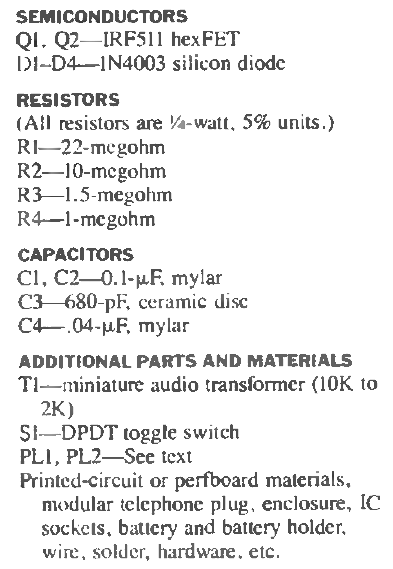
These are used to construct the foundation of an interface circuit for linking a cassette recorder to the phone line. This circuit provides more storage for the phone recording system which often become full due to unwanted sales pitches.
Once the interface circuit is deployed, you have to place a long play tap in your cassette recorder, hit the record switch and retrieve all the incoming messages.
Alternatively, the circuit can function as a 24-hour automatic secretary to record all the receiving phone calls.
Since operating power is supplied from the telephone line itself, a power supply is not needed for this circuit. The incoming signal is supplied across a bridge-rectifier circuit, comprising diodes D1 to D4.
If you are acquainted with the process of bridge rectifiers, you’ll know that the bridge warrants that no matter how the FET circuit is connected to the phone lines, the voltage at the junction of R1 and R3 are always positive.
When the phone is down, the voltage at the output of the bridge (at R1/R3 junction) is around 48 V. This voltage is supplied across a voltage divider comprising R1 and R2.
The voltage at the junction made of R1 and R2 is supplied to the gate of Q1. This action turns it on and allows the drain of Q1 to be pulled to low. Since the gate of Q2 is attached to the drain of Q1, the bias applied to the gate of Q2 is low, retaining it in the off state.
Once the answering machine returns to a call or the phone is lifted, the voltage across the phone lines drops below 10 V, allowing Q1 to turn off. At that stage, the voltage at Q1’s drain starts to escalate which turn Q2 on.
The remote input of the cassette is attached to Q2’s drain and source via S1 and a miniature plug chosen to connect with the remote input jack.
Switch S1 should be placed in a position so that the positive lead of the recorder’s remote input connects (through switch position 1) to Q2’s drain, and the negative input to Q2’s source.
Switch S2 delivers an easy method to reverse the circuit’s trigger output without the need to unsolder and re-solder the leads. The phone’s audio is connected through C1, C2 and T1 to the microphone input of the cassette recorder.
Sound-Activated Switch
In this last circuit as displayed in Figure below, the power FET is utilized a s switch in a sound-triggered cassette-recorder circuit.

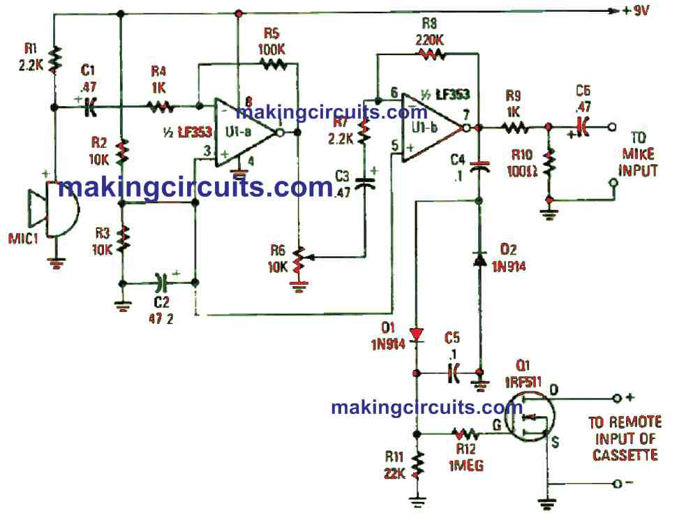

You may be able to find this type of circuits in a project for recording intermittent noise or wildlife sounds autonomously without having the recorder working continuously.
A sensitive electret microphone picks up the sound and supplies the signal to a two-stage amplifier circuit which comprises U1-a and U1-b.
The amplifier output of U1-b is delivered to a voltage doubler circuit (constructed of D1, D2, C4 and C5). The doubler’s output is actually the input to the gate of Q1. When the DC voltage meets the gate’s threshold level, Q1 will turn on and begin the recorder.
The cassette’s internal or external microphone can be deployed to recorded standard sound levels.
However, to detect weak sounds, you have to utilize the amplified output for an enhanced level. The circuit’s sensitivity is governed by resistor R6 and you can experiment this level to obtain the most optimum value.
MOSFETs are perfect components to use in high-voltage circuits thanks to it is protected against secondary voltage breakdown, unlike the usual power transistor.
You can also match any number of MOSFETs in parallel connections without needing a special high-wattage, current-matching resistor.
FET High Voltage Ignition
In Figure below, an IRF731 hexFET functioning as a high-current switch in a high-voltage generator ignition circuit is shown.

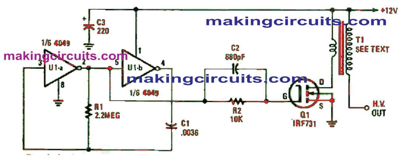


A pair of gates of a 4049 hex-inverting buffer (U1-a and U1-b) are configured as a typical squarewave-generator circuit. At pin 2 of U1-b, the output of the square wave generator (a narrow positive pulse) is applied.
This is then supplied to the gate (G) of Q1 via an R/C combination (comprising R2 and C2) that causes it to switch on and of at the same rate.
The fast switching current via the primary of T1 is changed into high voltage at T1’ secondary. Extreme caution must be exerted here, and you must isolate all attached body parts away from T1’s output. The high-voltage output of T1 is strong enough to hedge from the output terminal to one or both primary terminals.
When you need to operate the high-voltage circuit for any duration, always remember to use a heat sink with a minimum area of 9 in2 to be attached to Q1.
Alternatively, you may also equip with a piece of scrap aluminium. This FET circuit can function with an input voltage of up to 16 V for a short interval for higher output voltages.