


In this post we discuss the method for making a simple transformerless H-Bridge Inverter Circuit Using IC IRS2453(1)D and a few associated passive components.
Among the various pre-existing inverter topologies, the full bridge or the H-bridge topology is undoubtedly the most effective and successful. Configuring a full bridge topology could possibly require a great number of criticality, nevertheless with the introduction of full bridge driver ICs most of these have at the moment grown to be the least complicated inverters anybody can construct.
Full bridge inverter circuits also known as the H-bridge inverter, are the really economical types as these never rely on a center tapped transformers yet still have the ability to work with the proposed push-pull abilities right across the whole primary winding of the connected tansformers.
This characteristic makes it possible the application of smaller transformers and purchase more power outputs simultaneously.
Nowadays as a result of the hassle-free accessibility to full bridge driver ICs conditions have turn out to be totally hassle-free and manufacturing a full bridge inverter circuit at your home is now a kids fool around.
At this point we talk about a full bridge inverter circuit making use of the full bridge driver IC
from International Rectifiers.
The described chip is a remarkable full bridge driver IC because it single handedly looks after all of the the leading criticality associated with H-bridge topologies by means of its leading-edge integrated circuitry.
The assembler basically requires to connect a couple of several elements externally for accomplishing a full fledged, functioning H-bridge inverter.
The straightforwardness of the modelis indisputable from the diagram demonstrated below:
Pin14 and pin10 are the high side floating supply voltage pinouts of the IC. The 1uF capacitors in effect maintain these critical pinouts a tint more than the drain voltages of the respective mosfets making sure that the mosfet source potential remains below the gate potential for the preferred conduction of the mosfets.
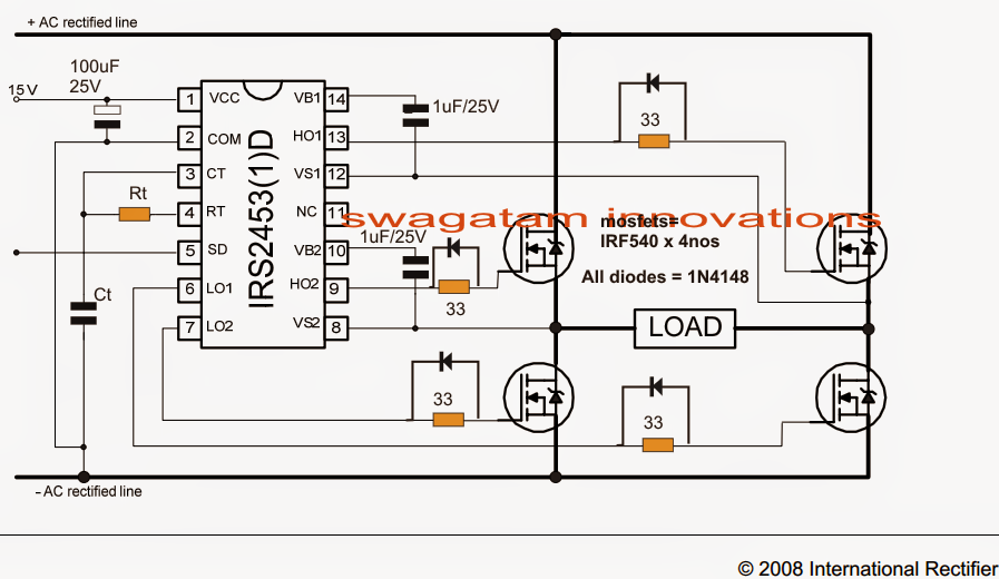
The gate resistors eliminate drain/source spike probability by stopping sharp conduction of the mosfets.
The diodes across the gate resistors are established for effective discharging of the inner gate/drain capacitors in the course of their nonconduction intervals for guaranteeing maximum reaction from the units.
The IC IRS2453(1)D is furthermore showcased with an integrated oscillator, which means simply no external oscillator stage may be necessary using this type of chip.
A few exterior passive parts manage the frequency for operating the inverter.
Rt and Ct could be determined for finding the required 50Hz or 60 Hz frequency outputs over the mosfets.
The following equation could be used for determining the amounts of Rt/Ct for the discussed H-Bridge Inverter Circuit Using IC IRS2453(1)D:
f = 1/1.453 x Rt x Ct in which Rt is in Ohms and Ct in Farads.
An additional fascinating characteristic of this IC is its potential to tackle extremely high voltages upto 600V rendering it flawlessly qualified for transformeless inverters or stream-lined ferrite inverter circuits.
As can be viewed in the presented diagram, in case an externally approachable 330V DC is implemented across the "+/- AC rectified lines", the arrangement straight away results in being a transformerless inverter whereby any expected load may be associated straight across the points imprinted as "load".
On the other hand in case a regular step-down transformer is employed, the primary winding could be associated across the points marked as "load". In this instance the "+AC rectified line" could be coupled with pin#1 of the IC and ended universally to the battery (+) of the inverter.
In case a battery greater than 15V is employed, the "+AC rectified line" has to be attached straightly with the battery positive whilst pin#1 ought to be carried out with a stepped down adjusted 12V from the battery supply applying IC 7812.
Despite the fact that the above demonstrated transformerless Inverter Circuit Using IC IRS2453(1)D appears to be extremely convenient to develop, the format involves certain stringent strategies to be adopted.
Transformerless UPS/Inverter Circuit
The post discuses an easy transfomerless 220 V to 220V DC online UPS inverter circuit.

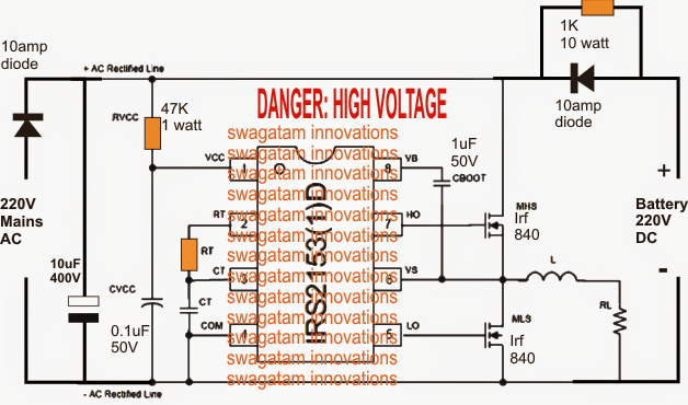
A relatively easy design might be noticed in the above diagram for the offered 220V DC UPS inverter circuit. Due to the IC IRS2153 from International Rectifiers which contains almost everything included inside one package for the essential execution..
Fundamentally, the IC is a qualified half bridge mosfet driver unit possessing all the essential safety limitations built-in, in order that we never must hassle concerning these while developing a customized half-bridge transformerless inverter circuit.
As can be watched in the diagram, there may be rarely anything difficult, it's just about establishing the mains input and an equivalently rated battery at the other side for developing a trouble free 220V online UPS circuit which happens to be solid state in design, noiseless, and transformerless topology.
The Rt and Ct are correctly elected for acquiring the essential 50 or 60Hz frequency for the output load.
It could be performed by making use of the following formula:
f = 1/1.453× Rt x Ct, where Ct will probably be in Farads, Rt in Hz, and f in Hz.
L1 could be picked with some testing to ensure the square wave harmonics could be regulated to a few preferred level.
The following, to prevent problem an automatic over charge cut off element is not involved, instead a trickle charge aspect is preferred charging the battery. This will likely take a pretty longer time for the battery to get charged but the problems of over charge is removed and diminished to safe levels.
The 1K 10 watt resistors signifies the charging rate for the battery, optionally the battery could be charged by way of a perfect external charger circuit