

In this post we comprehensively discuss how a zener diode works, its internal characteristics, zener breakdown voltage, its application method and how to connect zener diodes as voltage regulators
Working Principle of Zener Diode
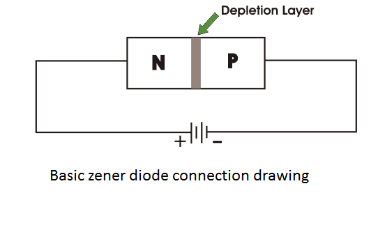
Whenever a PN junction diode is reverse biased, the depletion layer results in being wider. In case this kind of reverse biased voltage throughout the diode is raised consistently, the depletion layer will become a lot more larger. Simultaneously, you will see continuous reverse saturation current as a result of minority carriers.
Soon after particular reverse voltage over the junction, the minority carriers acquire adequate kinetic energy because of the formidable electric field.
Free electrons having adequate kinetic energy clash with immobile ions of the depletion layer and hit away a lot more free electrons. These types of freshly created free electrons additionally acquire ample kinetic energy because of the identical electric field, plus they generate considerably more free electrons by impact cumulatively.
For this reason commutative occurrence, pretty shortly massive free electrons will be produced within the depletion layer, and the whole diode will turn out to be conductive. This kind of breakdown of the depletion layer is called avalanche breakdown, however this breakdown is not really well-defined. There is certainly a different type of breakdown in depletion layer which can be sharper in comparison to avalanche breakdown, and this is referred to as Zener breakdown.
Whenever a PN junction is diode is extremely doped, the quantity of impurity atoms is going to be rich in the crystal. This increased quantity of impurity atoms leads to the greater amount of ions in the depletion layer consequently for very same applied reverse biased voltage, the thickness of the depletion layer results in being slimmer compared to that in a commonly doped diode.
For this reason slimmer depletion layer, voltage gradient or electric field strength throughout the depletion layer is fairly large. If the reverse voltage is sustained to increase, from a particular applied voltage, the electrons through the covalent bonds inside the depletion region emerge and create the depletion region conductive. This particular breakdown is referred to as Zener breakdown.
The voltage in which this breakdown takes place is referred to as Zener voltage. When the applied reverse voltage throughout the diode is greater than Zener voltage, the diode offers a conductive route to the current through it therefore, you cannot find any possibility of additional avalanche breakdown in it.
Hypothetically, Zener breakdown takes place at reduced voltage stage than avalanche breakdown in a diode, specifically doped for Zener breakdown. The Zener breakdown is significantly crisper compared to avalanche breakdown. The Zener voltage of diode may get altered in the course of manufacturing by using necessary and appropriate doping.
Each time a zener diode is attached across a voltage source, and the supply voltage is higher than Zener voltage, the voltage around a Zener diode stay fixed regardless of the source voltage. Eventhough at that situation current through the diode could be of any value based on the load associated with the diode. For this reason we utilize a Zener diode primarily for controlling voltage in various circuits.
Zener Diode Circuit

Zener Diode is simply an individual diode attached in a reverse bias, we have previously explained that.
A diode attached in reverse bias situation in a circuit is displayed above.
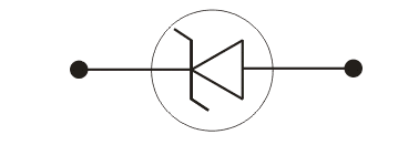
The circuit symbol of a Zener diode is additionally displayed below.

Now, talking regarding the diode circuits we have to examine the visual manifestation of the operation of the zener diode. Typically, it is referred to as V-I attributes of a Zener diode.
Characteristics of a Zener Diode
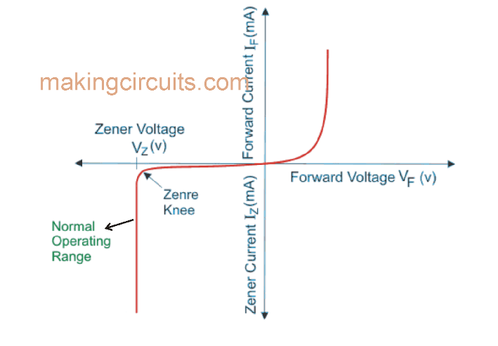

The earlier mentioned diagram exhibits the V-I attributes of a zener diode. When the diode is hooked up in forward bias, this diode functions like a regular diode however as soon as the reverse bias voltage becomes higher than zener voltage, a well-defined breakdown develops. Within the V-I characteristics above Vz is the zener voltage. Also, it is the knee voltage since at this moment the current boosts extremely quickly.
Zener Breakdown
A p-n junction is created by delivering p-type semiconductor content in contact with the n-type semiconductor content and they are recognized with regards to its depletion region. This is due to the width of the depletion area may differ according to the bias implemented across the terminals, determining the V-I characteristics of the p-n junction (Figure 1). The duration of the depletion region can be a function of either the employed bias along with the amount of doping.
It is observed that in the forward bias situation, the width of the depletion area minimizes with the escalation in the applied voltage that ultimately results in a rise in the quantity of current circulation. Alternatively, when the p-n junction is reverse biased, a rise in the applied voltage enhances the width of the depletion area.
Nonetheless, possibly you will see a small quantity of current move through the semiconductor because of the minority charge carriers. Additionally the width of the depletion area is witnessed to become narrow for intensely doped semiconductors and broad for softly doped semiconductors.


At this point, think about a heavily doped semiconductor afflicted by the reverse bias situation. Here the width of the narrow depletion area (because of high doping) is observed to extend with increased in the voltage employed across its terminals. This results in a rise in the electric field produced along the p-n junction since the electric field is simply the negative potential slope. For instance, a reverse voltage of 3V over a 100 Ao thick (incredibly narrow) depletion area produces the output of V/m electric field.
Because of this extremely heightened electric field, some of the covalent bonds in the p-n junction break-off liberating their valence electrons. This kind of free electrons could possibly get excited and proceed inside the conduction band resulting in an sudden upsurge in the current flow in the component. This occurrence is known as Zener Breakdown and the affiliated voltage is known as Zener Breakdown Voltage (VZ),
demonstrated in red color in Figure 1. The occurrence was initially detected and revealed by Dr. Clarence Zener in 1934 and is therefore named after him.
Further more it is to be taken into consideration that the Zener effect is really a adjustable trend since the amount of charge carriers created could be successfully manipulated by governing the electric field employed. Generally Zener breakdown brings about the diode junctions to breakdown under 5V and may not deteriorate the unit except if there is absolutely no provision made to discharge the heat produced.
Additionally, the Zener breakdown voltage offers negative temperature coefficient which means the Zener breakdown voltage minimizes with the increase in the junction temperature. On the other hand, it is to be taken into consideration that the voltage where the Zener breakdown takes place is variable throughout the device production. Last but not least it must be taken into account that the functioning of popular Zener diode is centered upon the Zener effect.
Application of Zener Diode
All of us understand what is Zener diode and what is the fundamental theory of operation of it. At this point the concern arises just where such type of diodes are employed. The primary implementation this type of diodes can be seen as voltage regulator, Over voltage protector, as voltage reference. We have reviewed the application of zener diode as voltage regulator, currently we are going to talk about additional two points in short ,. Overvoltage protection is performed by utilizing Zener diodes as there is current moving in the diode as soon as the reverse bias voltage surpasses a specific value.
This circuit gives basic safety for the device attached to the terminals. Typically the current must not go beyond standard valve, however in case on account of any error in the circuit the current surpasses the absolute maximum permitted limit, the device of the program could get destroyed permanently. An SCR is used, because of it the output voltage is rapidly decreased and a fuse bursts of disconnecting the input supply electricity. The circuit set up is displayed below for better comprehending.


Zener Diode as Voltage Regulator
Voltage references decide the constant supply of power, current or voltage as the zener voltage operates within a constant current supply. This is to prevent unpredictable overall performance, zener diodes are used where voltage reference is necessary like ohmmeters, ammeters and voltmeters.
Zener Diode as Voltage Regulator
The term regulator implies something that controls or regulates. Zener diode can function as a voltage regulator when it is presented in a given circuit. The output along the diode is going to be constant. It is driven with a current source. We all know that in case the voltage across the diode is greater than a specific value it may well draw abnormal current from the source. The basic diagram of zener diode as voltage regulator is presented under:
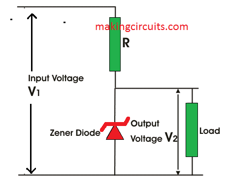

To restrict the current via the Zener diode series resistance R is brought in whose value could be picked from the given equation:


The aforementioned diagram is actually of a shunt regulator since the controlling component is parallel to the load. The Zener diode generates a well balanced reference voltage throughout the load that fulfils the requirements of the regulator.
Zener Diode as Voltage Regulator
A Zener diode is among the specifically developed diodes that mainly functions in reverse biased circumstances. These are a lot more intensely doped compared to normal diodes, because of which they possess narrow depletion area. While normal diodes may get destroyed if the voltage across them surpasses the reverse breakdown voltage, Zener diodes do the job specifically in this area. The depletion region in Zener diode extends back to its standard state as soon as the reverse voltage is eliminated. This specific property of Zener diodes causes it to be beneficial as a voltage regulator. We will learn how this takes place.
Let us first of all understand how a Zener diode functions prior to understanding Zener diode as a voltage regulator.
Characteristics of a Zener Diode
Once we apply a reverse voltage to a Zener diode, a minimal level of current runs via the circuit. If a voltage beyond Zener breakdown voltage is employed, Zener breakdown takes place. Zener breakdown is an occurrence in which a considerable level of current streams through the diode that has a minimal drop in voltage.
Whenever we raise the reverse voltage even further, the voltage over the diode continues to be at the exact same value of Zener breakdown voltage although the current through it continues to climb as may be observed in the graph above. Within the graph Vz relates to the Zener breakdown voltage. Zener breakdown voltage normally can vary from 1.2 V to 200 V based on its application.
A fantastic aspect of this diode is that we are able to choose the Zener diode having a appropriate breakdown voltage to function as a voltage regulator within our circuit. As an example, suppose we would like that the voltage around a load in our circuit doesn't go over, let’s say, 12 volts. In that case we are able to select a Zener diode with a breakdown voltage of 12 volts and hook up it along the load. After that even if the input voltage happens to go over that value, the voltage across the load would not go beyond 12 volts.
We will make an effort to comprehend that using a circuit diagram
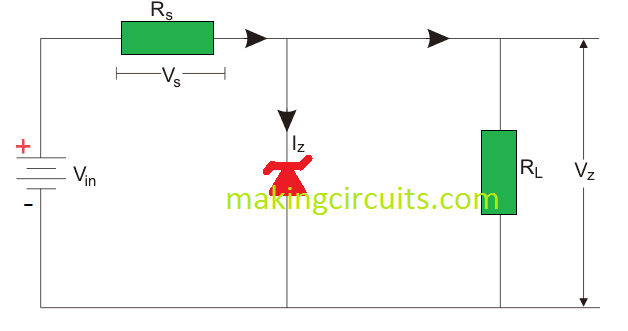

Here the Zener diode is attached across the load RL. We would like the voltage across the load to be governed and never surpass the value of Vz. Based on our condition, we opt for the suitable Zener diode having a Zener breakdown voltage in close proximity to to the voltage we call for across the load. We hook up the Zener diode in reverse bias situation.
As soon as the voltage across the diode surpasses the Zener breakdown voltage, a substantial level of current begins moving through the diode. Because load is in parallel to the diode, the voltage drop throughout the load is likewise equal to the Zener breakdown voltage. The Zener diode offers a path for the current to stream and therefore the load becomes safeguarded from abnormal currents. Consequently the Zener diode helps a couple of objectives here: Zener diode as a voltage regulator in addition to it safeguards the load from extreme current.