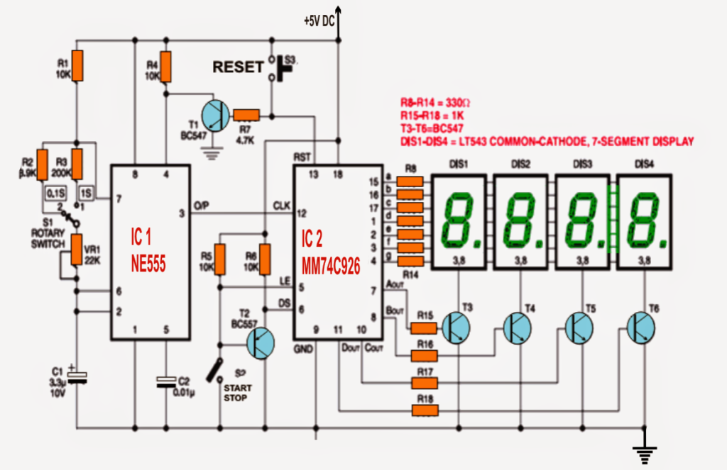
Presented below we shall analyze a digital stop watch design designed around the quite popular IC LM555 together with a 4-digit counter IC with multiplexed 7-segment output drivers (MM74C926).
IC MM74C926 is internally composed of a 4-digit counter, an output latch up level, a npn output liable for sourcing driver networks for common-cathode, 7-segment display and an internal multiplexing circuitry with four multiplexing outputs.
The multiplexing circuit level also consists of an in-built free running oscillator, and does not make use of any further external frequency creating network.
The counter is made to continue on a negative rising of the clock signals.
The clock signal is produced by the timer IC LM555 (IC1) and pleased over pin 12 of IC2.A higher signal on reset pin 13 of IC2 resets the IC to zero logic.
Reset pin 13 is linked to +5V by using a reset push-on-switch S3.
The occasion S2 is is pressed even for a fraction of a second, the count figure is presented to a zero logic, transistor T1 acts with a trigger and it resets IC1.
This enforces the counting to commence in an incident whereby S2 is due to ‘off’ condition.
A low logic signal on the latch-enable input pin 5 (LE) of IC2 latches the count in the counter module into the on chip set output latches.
In an event when switch S2 is activated, pin 5 is driven to go low and thereby the count figure is able to be saved in the latch section of the IC.
Display-select pin 6 (DS) ascertains if the figure on the counter or the placed count in the latch could be revealed on the display or not.
In the event that pin 6 is held low the figure in the output latch section is empowered to get presented, on the other hand if pin 6 is provided with a high logic the count stored in the counter is activated over the hooked up display.
On an instance when switch S2 is changed, the base of pnp transistor T2 is attached to ground to be certain that it starts functioning. The emitter of T2 is rigged with DS pin of IC2.
Therefore, the moment switch S3 is activated, reset pin 13 of IC2 is put together with negative by way of the transistor T1 ensuring that the oscillator is inhibited from developing clock pulses. This performance is carried out to put into practice a synchronization between IC1 and IC2.
At the first phase, reset the module that allows you to permit the display to indicate ‘0000.’ Following disconnect switch S2 for the stop watch to cause its counting the periods. In the event you wanted to reduce the clocking of the chip, simply shut off the control S2.
The provided rotary switch S1 could be preferred picking the a variety of time intervals at the output of the astable multivibrator (IC1).
The design will continue to work off a 5V supply inputs. The circuit could be conveniently fitted and constructed on a general-purpose PCB.
It is important to enclose the complete circuit in a metallic cabinet with slots built for four 7-segment displays, rotary switch S1, start/stop switch S2 and reset switch S3 in the dashboard plate of the picked encloser.
