

Perhaps you have had desired just one single more logic gate or an logic inverter stage to complete that specific circuit design? Or you may at times realize that an inverter or gate is absent in the output stage? In such situations, how would you consider one of the following basic add-on circuits, designed using discrete transistors, to complete that emptiness?
In the following circuits we learn how to make simple logic equivalent inverter and buffer amplifier stages using discrete BJTs.
Logic Inverter Stage using BJTs
The circuit as depicted in Figure below is a standard inverting amplifier that can be powered from most CMOS of TTL ICs. The truth table for this circuit is quite similar as what one would expect from a common integrated-circuit logic inverter. In short, high in, low out; low in, high out.

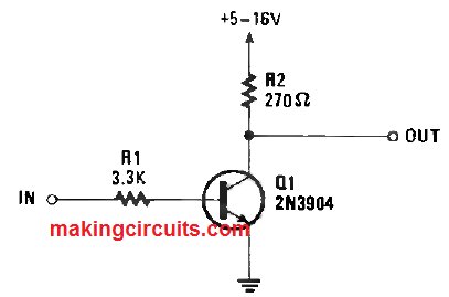
When the output of the BJT inverter is high, it will channel the drive current which is restricted only by the value of R2 and the transistor to whatever circuit network that is attached to its output. Once the inverter’s output goes low, the attached circuit network which is connected to its output will be arrested to ground. The magnitude of current the transistor can sink relies on its gain and power modulating capabilities.
Non-Integrated Discrete Buffers
The circuit in the following figure shows a BJT equivalent of logic non-inverting amplifier and buffer stage that can be utilised to elevate output drive current. The truth table shows that a high input delivers a high output, whereas a low input provides a low output.


Not quite same like the last circuit, this one is a little complicated. Hence, we will describe the circuit a little. Once a positive input is applied to Q1’s base, it switches the transistor on, pulling the base of Q2 low and turning Q2 on. Simultaneously, the low at Q1’s collector is also applied to the base of Q3 which causes it to switch off. This means that the circuit’s output is the supply voltage sans the voltage drop identified across Q2 and R4.
When the input is low, Q1 and Q2 are switched off. Once Q2 is off, it will not sink any current from its output. Furthermore, if the circuit has a driver whose connection needs the load to be arrested to ground, transistor Q3 must be added. With Q1 switched off, its collector becomes close to the supply voltage. This then delivers bias to Q3 which turns it on and locks the output to ground. Bias is removed from Q3’s base when Q1 switches on. This action turns off and locks the output.