

In a simplistic manner, the triac can be considered as a switch control. When it is in a blocked state, it behaves like an open switch. However, a command current applied to the triggering electrode of the triac leads to its conduction. Its behavior is then that of a shorted switch. In the absence of a command current, the triac systematically switches from a conductive state to a blocked state during the alternating transition of the AC input.
Structure of a triac:
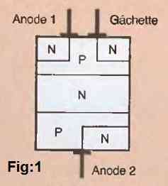
The triac can be assimilated to two thyristors connected in parallel (anti-parallel association) and thus constitutes a bidirectional element. Figure 1 shows the structure of this semiconductor.

Operation of a triac:
A triac can transition from a blocked state to a conductive state if a trigger current passes through the gate or if the voltage between its A1 and A2 electrodes exceeds a certain value (in practice, this occurs due to some voltage spikes in the power supply causing unintentional triggering).
A triac returns to the blocked state following a reversal of the polarity voltage between its A1 and A2 terminals or when the main current falls below the value of the holding current Iu.
The triggering of a triac:
In an alternating supply, a triac can be triggered in both directions of polarization of its main electrodes A1 and A2. Thus, according to the polarization of the trigger current, four quadrants of polarization of the triac are defined (Figure 3).

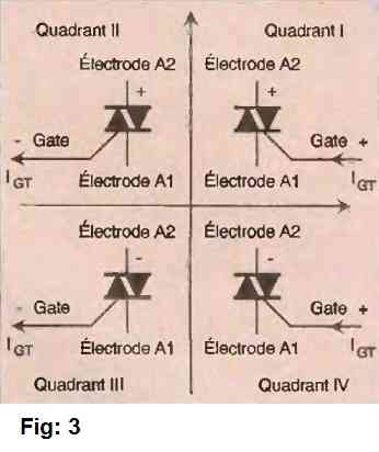
Each quadrant corresponds to a mode of triggering the triac. These modes are summarized by the simplified notation table in Figure 4.

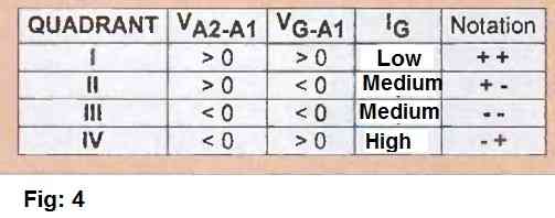
For example, if a voltage VA2-A1 > 0 is applied between the main electrodes of the triac and a negative gate voltage is applied relative to the anode A1, the triac is polarized in quadrant II, denoted as +-.
For each triggering quadrant, an IGT trigger current, an IH holding current, and an IL latching current are defined. The trigger current must be maintained until the main current has exceeded the holding current IH by two to three times. The minimum trigger current is the triac's latching current IL.
Once the gate current is removed, the triac remains conductive as long as the anode current is greater than the holding current IH. Depending on the quadrant, triggering the triac may be more or less difficult, especially for quadrant IV, which generally requires a trigger current twice as large. In practice, quadrant IV is generally avoided.
Furthermore, there are two main families of triac control modes II and III, which are defined by the circuit diagram shown in Figure 6, where a negative gate current is applied.

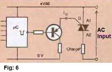
Figure 7 shows a typical application of Triac control in modes II and III. When transistor T is blocked, capacitor C is charged through resistor R2 and diode D1. This diode prevents the capacitor charging current from flowing through the Triac gate.

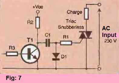
A Schottky diode is preferable for this purpose as it has a low forward voltage drop, ensuring a voltage lower than the Triac gate trigger voltage (VGT). When transistor T1 becomes conductive, capacitor C1 is charged through the Triac gate circuit, leading to conduction. The gate current is thus a negative current pulse passing through resistor R1 and transistor T1.
The figure 7 presents a snubberless application of a Triac controlled in modes II and III. When the transistor T is blocked, the capacitor C is charged through the resistor R2 and the diode D1.
This diode prevents the discharge current of the capacitor from going through the Triac gate. A Schottky diode model is preferred because its low forward voltage drop guarantees a voltage lower than the VGT voltage of the Triac gate.
When the transistor T1 becomes conductive, the capacitor C1 is charged in the Triac gate circuit, causing conduction. The gate current is thus a negative current pulse passing through the resistor R1 and the transistor T1.
Constraints of use:
The Triac has some constraints of use, particularly in the case of inductive loads or surrounding parasites. These constraints relate to the speed of voltage variation (dV/dt) between the Triac anodes and the dl/dt of the main current.
Indeed, when the Triac switches from the blocked state to the conductive state, a significant current may be caused by the external circuit. At the same time, the voltage drop across the Triac is not instantaneous.
Consequently, there will be simultaneous presence of voltage and current resulting in instantaneous power that can reach significant values.
The energy dissipated in a small space results in a sudden elevation of the junction temperature. If the critical thermal limit is exceeded, the Triac will be destroyed due to an excessive dl/dt.
The constraints of voltage variation are of two orders: the dV/dt applied to the blocked Triac and the dV/dt applied to the Triac in conduction (also called dV/dt in commutation).
Excessive decrease in the applied voltage between the A1 and A2 terminals of a blocked Triac risks triggering it in the absence of a gate signal. This phenomenon is due to the charging of the Triac's internal capacitance.
The discharge current of this capacitance can be sufficient to trigger the Triac, but this is not the main risk of unwanted triggering.
The maximum value of the Triac's dV/dt in commutation is generally much lower, and too rapid variation in voltage across the Triac at the moment of its blocking can also cause a new triggering. The Triac is thus turned on when its blocking is sought.
RC network protection
An RC protection network for the triac, as shown in Figure 8, is often desirable to limit the effects of dV/dt and overcurrent, especially if the load is inductive or in the case of certain types of external surges.

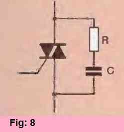
The calculation of the values of the components R and C depends on several parameters, including the value of the current in the load (inductance and resistivity of the load), the service voltage, and also the characteristics of the triac.
Since it is difficult to identify all of these parameters, empirical values are often used. The combination of a 100-150 Ohm resistor and a 100 nF capacitor gives satisfactory results.
However, it should be noted that the value of the resistor should be lower or of the same order of magnitude as the load while being high enough to limit the capacitor discharge current to respect the maximum value of dI/dt at the time of initiation.
Additionally, an RC network improves the conduction turn-on of a triac controlling an inductive load. The charge current of the capacitor, in fact, makes up for the delay in the initiation of the inductive current by keeping the main current above the minimum holding value IH.
Additional protection measures for triacs.
One such measure is to add a varistor in parallel to the supply voltage, which will attenuate the parasitic voltage spikes on the power line.
Newer triacs, called SNUBBERLESS or Hi-com triacs, are designed to operate without an RC protection network and have improved dV/dt and di/dt characteristics, particularly during commutation.
These triacs are designed for use with inductive loads such as motors, coils, and relays. However, they are not recommended for use in quadrant IV and are only suitable for quadrants I, II, and III. STMicroelectronics offers Hi-Com triacs with the suffixes CW or BW for the most advanced models.
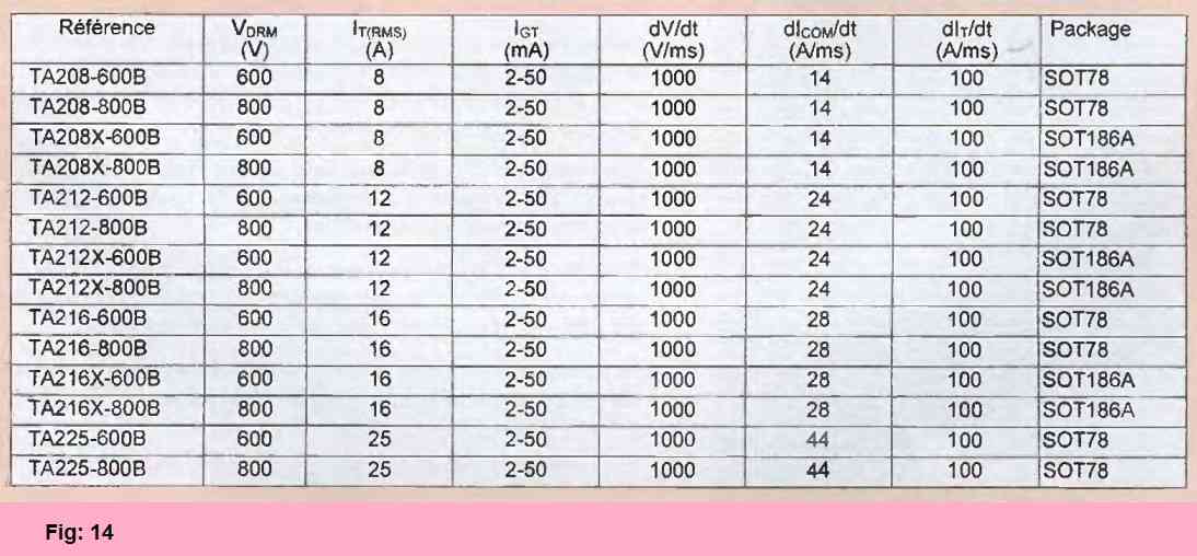
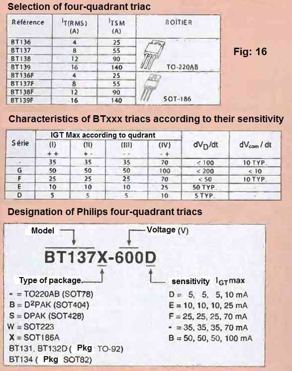
The selection table in Figure 14 shows a range of Hi-Com triacs from Philips Semiconductors. In some cases, it may be necessary to improve the protection of these triacs, especially in the off-state.

For example, a TRANSIL or a varistor can be used to limit the voltage spikes caused by parasites, and an RC network can also be used to attenuate the dV/dt. The components used in this case can be smaller and less expensive than those used in a protection network for a standard triac.
Sensitive Triacs
Sensitive triacs for logic circuits are triacs that are sensitive to current, with an activation current generally lower than 5 or 10 mA depending on the series (TW and SW for STMicroelectronic products and D and E for Philips Semiconductors).
The TLC series from STMicroelectronic is an old design of sensitive triacs that is now obsolete. Most microcontrollers or other logic circuits can directly command these triacs.
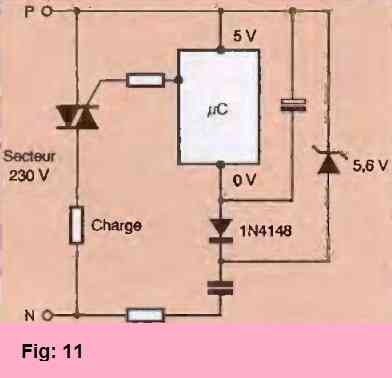
Due to their ease of use, they are ideal for projects that require a small number of components, such as controlling lamps, heating resistors, or small motors. Figure 11 illustrates such an application with a low-voltage direct supply from the mains.

List of Triacs
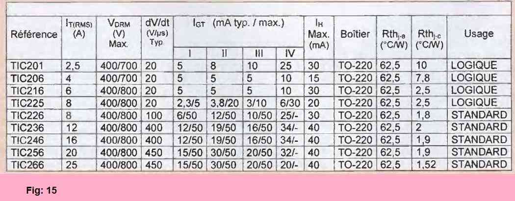
There are numerous manufacturers of triacs, but a few references are familiar on the consumer market. The MO tables below, along with Figures 15 and 16, complete the selection of the main triacs encountered among the various suppliers.


Main Characteristics
The main characteristics are defined below:
- Irowsi: Effective current in the on-state of the triac
- Irsu: Surge current of accidental point in the on-state of the triac
- It: Holding current in the on-state of the triac
- Iows: Latching current in the off-state of the triac
- Igt: Gate trigger current
- IH: Latching current
- Vgt: Gate trigger voltage
- VDRM: Repetitive peak voltage in the off-state
- dV/dt or dV/dt: Critical rate of rise of voltage at the off-state
- dl/dt: Critical rate of rise of current at the on-state
- di/dt: Critical rate of fall of current at the off-state
- tm: Gate controlled turn-on time
- Rthi: Junction-to-case thermal resistance
- Rthj-a: Junction-to-ambient thermal resistance
Summary of the main uses of triacs:
-To turn on a triac, a current exceeding the maximum value of IGT must be applied to its gate. This current must then be maintained until the main current passing through the triac reaches the value of IL. To return the triac to its blocked state, the main current passing through the thyristor must drop below the value of IH for a sufficient amount of time.
-When designing a triac circuit, it is strongly recommended to avoid triggering the triac in quadrant IV (IGT>0 and VA2_A1<0).
In addition, new generations of triacs are not usable for source IV triggering mode. Precautions must be taken to avoid disturbances due to environmental parasites, especially if the triggering circuit is connected to the triac by wires.
In this case, the wires should be of a minimum length, and preferably twisted pair or shielded cable should be used. A resistance of 1 kΩ or less should be placed in parallel between the gate and electrode A1. A low-pass RC filter can complete the protection.
-If there are unwanted triggerings, triac protection must be put in place. If dV/dt or (dV/dt)COM are critical, an RC network in series between the anode and cathode is necessary. If dl/dt is limited, a self-inductor of a few microhenries should be placed in series with the load. A better alternative is to use new-generation triacs such as snubberless or Hi-Com triacs.
-If the repetitive peak voltage at the blocked state of the thyristor VDRM is excessive due to parasitic voltage spikes, a self-inductor of a few microhenries in series with the load should be placed.
A varistor in parallel on the 230V sector can complete the mains filter and protect the thyristor. A gate current strong enough, within the limits of the triac characteristics, is recommended to maintain the triac characteristics over time and prevent a progressive degeneration of its gate circuit.
-In case of extreme dl/dt, a self-inductor of a few microhenries or a CTN thermistor should be placed in series with the load.