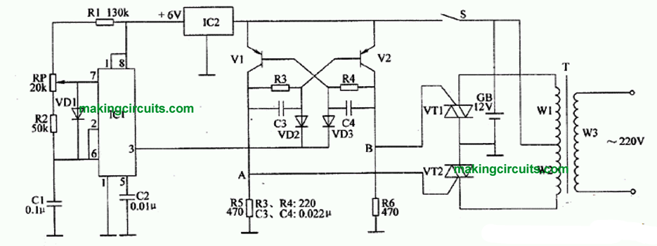
The first IC 555 inverter circuit with triacs makes use of an IC 555 for generating the oscillations and triacs for converting these oscillations into mains voltage through the transfomer.
The IC 555 is configured in it normal astable multivibrator mode for generating the required 50 Hz oscillations, and remember these oscillations can also be customized by adding a PWM pot with the IC 555 configuration.
OK, next the oscillation from the pin#3 of the IC 555 is given to a transistor flip flop stage using V1, and V2 which transforms the alternating high and low logics from the IC 555 into alternating flip flop pulses for the output power devices.
The output power devices here are not configured around power BJTs, mosfets, IGBTs rather ordinary triacs with the transformer.
Using triacs eliminates the restriction of having low secondary voltage transformers and allows higher voltage transformers such as 48-0-48V, or even 100-0-100V transformer which further means huge reduction in battery current and enabling compact inverter size even with high wattage designs.
The output from the V1, V2 stage is appropriately fed to the triac gates which instantly begin oscillating at the specified frequency.
The transformer can be any rated depending on the battery power and the load requirement.
No, the triacs would not latch even though this IC 555 inverter circuit using triacs operates with DC, because the two triacs react on the two winding of the transformer which generate back EMFs which are opposite to the other triacs and instantly breaks the conduction for the triac which is not in the triggered mode.

Parts List
- IC1 is IC555
- V1, V2 = 2n2907
- all diodes are 1N4007
- R3, R4 = 27K
- C3, C4 = 470nF
- IC2 = 7806 IC
- VT1 = 8amp/400V triacs
- transformer= 30-0-30V/10amp
- battery = 36V/25AH
- wattage output = 300 watt
Simple Full-Bridge Inverter Circuit using IC 555
In the second design we are going to study a simple full-bridge inverter circuit using IC 555, which can be built by any new hobbyist within few hours and see it running successfully.
What is Full Bridge Inverter
A full bridge inverter is also referred to as an H-bridge inverter circuit usually requires a relatively complex circuitry for accomplishing its working conditions. It cannot be achieved through simpler means because this type of topology demands a two way push pull operation of the connected transformer, which is a two wire transformer and not a center tap one.
A full bridge topology is often the preferred topology and is quite popular because in this configuration the inverter works with only a single primary winding and is able to utilize it with maximum efficiency through a full end-to-end push-pull conduction of the winding.
This enables the transformer to be smaller and compact in size and yet deliver better efficiency compared to the center tap topology where only 50% of the primary is utilized during each magnetic switching cycle, which results in a 50% less efficiency than a full bridge counterpart.
Normally it is thought that full bridge inverter can be built only with special ICs or using complex circuit configurations. In this article we will try to figure out how a full bridge inverter can be built using a simple IC 555 circuit as shown below.
However this high efficiency full bridge topology comes with a drawback, here we have to employ two batteries instead of one. But two batteries also means higher amount of backup, so in fact two batteries become beneficial and not a drawback in the long run.

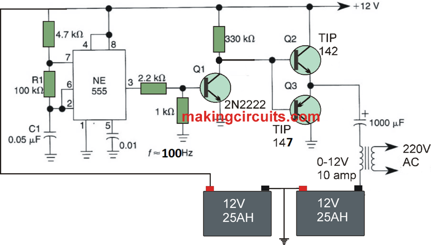
How the Circuit Functions
As you can see the shown IC 555 full bridge inverter circuit is extremely simple and yet is capable of delivering some serious amount of output power with a relatively smaller transformer
The IC 555 is rigged as a standard astable multivibrator, for generating a constant 100 Hz frequency at its pin#3.
This frequency is applied to a buffer transistor stage using 2N2222.
The collector of this buffer transistor is connected to a push pull driver power transistor stage using a couple of Darlington transistor TIP142 and TIP147.
The TIP142/147 are high gain Darlington power transistors capable of supplying around 10 amp current to a connected load.
Here the load is in the form of transformer primary winding, and therefore the power BJTs deliver the full 10 amp across the primary of the transformer in a push pull manner, quite similar to a H-bridge inverter circuit.
You can also see a 1000uF/25V capacitor connected in series with the transfromer, this is to ensure that the power transistor do not get overdriven or overloaded under any circumstance and thus protect the BJTs from a catastrophic situation.
This capacitor also determines the maximum amount of current that can pass into the transformer and thus consequently decides the power rating of this Full bridge inverter circuit.
The user may feel free to increase the value of this capacitor in order to upgrade the power of this IC 555 based simple full bridge inverter circuit.
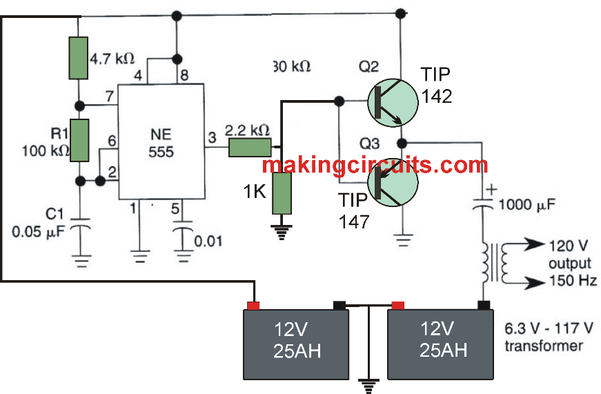
Simplifying the Circuit
A careful inspection of the circuit suggests that the BJT 2N2222 has no crucial role in the operation of the inverter and therefore can be simply eliminated.
The simplified version of the circuit can be witnessed below, which now looks a truly easy to build IC 555 H-bridge inverter circuit.

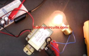
Prototype Circuit and Working Results