


A straightforward but yet greatly advanced IC TL494 PWM Modified Sine Wave Inverter circuit is offered in this article post. The application of the PWM IC TL494 not just causes the layout incredibly affordable with its components estimate but additionally remarkably efficient and precise.
The IC TL494 is an ideal PWM IC which is intended essentially to match all sorts of circuits which necessitate accurate PWM dependent outputs.
The chip possesses all the needed capabilities built-in for creating genuine PWMs which can be customized according to the customers utility specifications.
PWM Modified Sine Wave Inverter Circuit Employing IC TL494
In this article we talk about an adaptable IC TL494 PWM Modified Sine Wave Inverter which contains the IC TL494 for the vital sophisticated PWM reproduction.

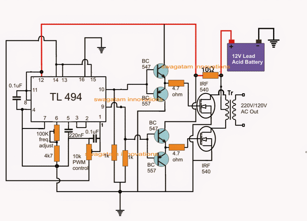
Looking at the picture above, the many pinout functions of the IC for executing the PWM inverter functions can be grasped with the following facts:
Pin#10 and pin#9 are the two outputs of the IC that happen to be organized to operate in tandem or in a totem pole arrangement, which means each the pinouts can never turn out to be positive collectively instead are going to oscillate alternately from positive to zero voltage, that would be once pin#10 is positive, pin#9 possibly will see zero volts and vice versa.
The IC is capable to deliver the above totem pole output by connecting pin#13 with pin#14 and it is the reference voltage output pin of the IC fixed at +5V. Consequently given that pin#13 is rigged with this particular +5V reference it enables the IC to generate alternately swapping outputs, nevertheless in case pin#13 is grounded the outputs of the IC is compelled to change in a parallel switching format (single ended mode), which means the two the outputs pin10/9 will start changing over collectively rather than alternately.
Pin12 of the IC is the supply pin of the IC which may be identified attached to the battery by means of a limiting 10 ohm resistors which filters out any specific potential surge or a turn on shoot up for the IC.
Pin#7 is the primary ground of the IC when pin#4 and pin#16 are grounded for certain stipulated reasons.
Pin#4 is the DTC or perhaps the dead time regulation pinout of the IC which decides the dead time or the space between the turn on intervals of the a pair of outputs of the IC.
By the manufacturer it will be hooked up to ground to ensure the IC produces the very least interval for the "dead time", but for accomplishing greater dead periods of time, this pinout could be provided with an external changeable voltage from 0 to 3.3V letting a linearly workable dead time from zero to 100%.
Pin#5 and pin#6 are the frequency pinouts of the IC which need to be associated with an outside Rt, Ct (resistor, capacitor) system for establishing the needed frequency across the output pinouts of the IC.
Either one of the two could be modified for altering the preferred frequency, in the suggested PWM modified inverter circuit we implement a adjustable resistor for empowering the alike. It might be fine-tuned for accomplishing a 50Hz or 60Hz frequency on pins9/10 of the IC in accordance with the conditions, by the individual.
The IC TL 494 offers a dual opamp network internally arranged as error amplifiers, that happen to be placed to rectify and dimension the output switching duty cycles or the PWMs in accordance with the usage technical specs, in ways that the output delivers precise PWMs and guarantees the best RMS personalization for the output stage.
The inputs of the error amplifiers are designed across pin15 and pin16 for 1 of the error amps and pin1 and pin2 for the subsequent error amplifier.
Usually a single error amplifier is employed for the highlighted automatic PWM set up, along with the other error amp is retained inactive.
As may be seen in the diagram, the error amp with the inputs at pin15 and pin16 is kept sedentary by grounding the non-inverting pin16 and by linking the inverting pin15 to +5V with pin14.
Therefore internally the error amp linked to the above pins keep on being non-active.
Nevertheless, the error amp possessing the pin1 and pin2 as the inputs are appropriately employed here for the PWM adjustment functioning.
The figure reveals that pin1 which happens to be the non-inverting input of the error amp is hooked up to the 5V reference pin#14, by means of a variable potential divider by means of a pot.
The inverting input is associated with pin3 (feedback pin) of the IC that may be in fact the output of the error amps, and makes it possible for a feedback loop to build up for pin1 of the IC.
The above pin1/2/3 arrangement makes it possible for the output PWMs to be establish precisely by modifying the pin#1 pot.
This concludes the main pinout application n guideline for the mentioned modified sine wave inverter using the IC TL494.
Currently for the output power stage we are able to see a few mosfets put into use, powered by a buffer BJT push pull stage.
The BJT stage guarantees perfect switching platform for the mosfets by presenting the mosfets with minimal spurious inductance problems and fast discharge of the internal capacitance of the fets. The series gate resistors protect against any transients aiming to create its route into the fet hence guaranteeing the procedures to be completely secured and effectual.
The mosfet drains are associated with a power transformer that can be a regular iron cored transformer owning a primary design of 9-0-9V if the inverter battery is evaluated at 12V, and the secondary could possibly be 220V or 120V in accordance with the user's country requirements.
The power of the inverter is essentially contingent on the transformer wattage as well as the battery AH specifications, one can possibly modify most of these variables in respect to personal preference.
To make a stream-lined IC TL494 PWM Modified Sine Wave Inverter, the iron core transformer could be swapped with a ferrite core transformer. The winding particulars for the same could possibly be noticed below:
By means of super enamelled copper wire:
Primary: Wind 5 x 5 turns center tap, choosing 4 mm (2 2 mm strands wrapped in parallel)
Secondary: Terminate 2000 turns of 0.5 mm
Core: any specific fitting EE core that would have the ability to contain these winding effortlessly.