

The post explains how to make a simple PWM amplifier circuit also called class-D amplifier or switching amplifier.
A PWM amplifier is an electronic amplifier in which the amplifying devices (transistors, usually MOSFETs) work as electronic switches, rather than as linear gain devices as in other amplifiers.
They function by quickly switching to and fro amongst the supply rails, being provided by a modulator using pulse width, pulse density, or related methods to encode the sound input into a pulse train.
The sound gets through via a easy low-pass filter into the loudspeaker. The high-frequency pulses are blocked.
Since the pairs of output transistors are never switching at the same time, there is absolutely no other path for current flow except from the low-pass filter/loudspeaker. Because of this, efficiency can reach over 90%.
Although a few initial teething troubles. Pulse Width Modulation (PWM) is known by many to be the alternative in sound circuit design.
Eventhough it provides merely a modest 3 watt output, it is a highly functional, precise and reliable amplifier.
The main topic of digital sound has long been handled prior to and will certainly be again.
The advantages are amazing, to the point that almost all important makers of sound devices are examining its alternatives.
Recording firms too know about the opportunities a digital system (digitally recorded records happen to be accessible commercially).
Until quite not too long ago, the efficiency of PWM amplifiers was dissatisfactory because of the low quality semiconductors utilized.
With the arrival of recent high speed switching transistors, PWM is currently emerging of age.
How the Circuit Works
To begin with a PWM amplifier includes a symmetrical squarewave generator.
The duty cycle of this squarewave is then modulated by the sound signals. The output transistors usually do not work linearly but work as switches, that is, they are either full ON or OFF.
Under quiescent circumstances the duty cycle of the output waveform is 50% meaning that every single output transistors is totally saturated (conducting) for an equal timeframe.
The average output voltage is therefore zero. It therefore follows that if one of the output switches is shut for a longer period than the other, the average output voltage will then be possibly negative or positive based on the polarity of the input signal.
It can be seen then that it is the average output voltage that is proportional to the input signal. Since the output transistors work solely as switches, very little power loss occurs in the output stage.
A self oscillating PWM amplifier is one in which the squarewave generator, the pulse width modulator and the output stage forms a single unit.
This developed a powerful amplifier with merely a very small amount of components. A version of this is certainly explained in this article.
The circuit of the complete amplifier is demonstrated in figure 1. It can be noticed that a PWM amplifier need not be quite difficult at all.

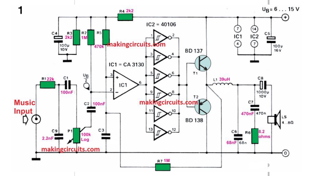
The input signal is fed to an opamp. IC1. This is used as a comparator and is accompanied by numerous Schmitt triggers in parallel.
This has two functions. First of all the waveform is required to be ' square ' and second of all adequate base drive current is required for the output stage which employs two ordinary but relatively quick transistors (BD 137/138).
The whole amplifier oscillates and creates a squarcwave. This is because one of the inputs of the comparator (IC1) is attached to the output through an RC network.
Both inputs of IC1 are biased to one half of the supply voltage making use of voltage divider R3/R4. Whenever the output of IC1 is low and the emitters of T1/T2 are high, capacitor C3 is charged in terms of R7 and the voltage increases at the non-inverting input.
If it increases above the level of the inverting input, IC1 ' s output changes low to high and the emitters of T1/T2 change from high to low. Because of this, C3 is currently released through R7, the voltage at the plus input falls below that of the minus input and the output of IC1 switches back to a low state.
The result is a squarewave output; the frequency of which depends on R7 and C3. The values provided lead to an oscillation at 700 kHz.
Presented Murphy fails to get in the way, we should come with an oscillator. Now we have to pulse width regulate it. The level at the inverting input of IC1, utilized as a reference, does not continue to be constant but depends on the sound signal.
The point at which the output of the comparator changes, is also dependant on the amplitude. Because of this the width of the squarewaves is constantly changed (modulated) by the sound signal At the output of the amplifier, filtering is needed; it is not meant to work as a 700 kHz transmitter! An LC/RC network is employed, including L1/C6 and C7/R6.
With a load of 8 ohms and a supply voltage of 12 volts, the amplifier developed 1.6 watts. At 4 ohms, 3 watts were measured. Cooling the output transistors was not essential.
The harmonic distortion turned out to be remarkably low for this type of easy design. Less than 0.32% total harmonic distortion from 20 Hz-20 kHz was measured.

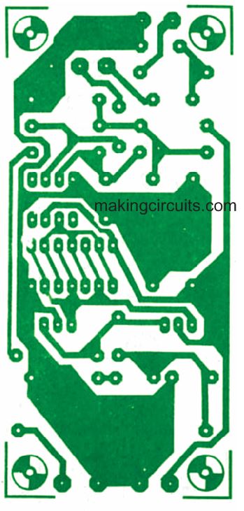

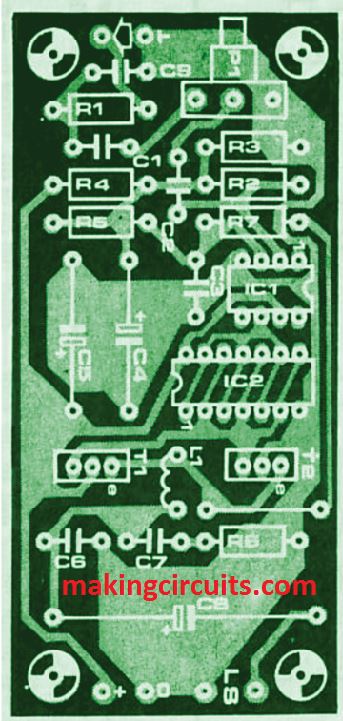
Figure 2 demonstrates the printed PWM amplifier circuit board and parts layout for the amplifier. Its construction demands short amount of time and money, so it provides an exceptional chance for anyone wishing to develop into much better familiar with PWM.
Another Simple PWM Amplifier Design
This simple circuit can be adapted to encode an audio signal into PWM, as shown in the diagram below. The music is directly added to the non-inverting input, which causes the threshold switching voltages to change. R5 and R6 both inhibit crosstalk between the audio stream and the carrier. DC voltages are isolated from the astable by capacitor C2.

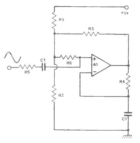
Unfortunately, because C1 charges exponentially via R4, R3 is substantially greater than R1 or R2, resulting in less hysteresis.
This causes the switching levels to be fairly close around each other, giving rise to the triangular waveform across C1 as a response of it being charged via R4. An LF351 op-amp is used to generate a better square wave at high frequencies. This is a high-slewing-rate VFET device, with a slewing rate of 13 V/uS.
The next Figure below depicts the digital amplifier's complete circuit. A couple of transistors in a push-pull output stage are driven by the op-amp.

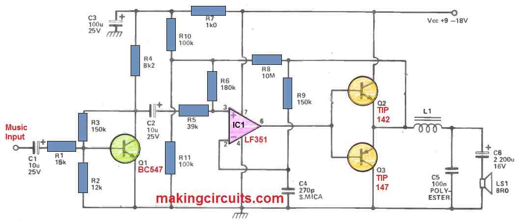
The collector current of these TIP142 and TIP147 transistors is 1 A. As you can see, they're coupled as emitter-followers, with no base bias. Q2 is saturated whenever the op-amp output is high, and it delivers current to the load through the low-pass filter L1, C5, and the output coupling capacitor C6. In class B amplifiers, the later component is frequently of reduced amount. This is unfortunate because the lower -3 dB point is determined by the capacitor's size. As you may recall, a capacitor's impedance Z could be determined by:
Z = 1 / 2 π FC
Where Z is in Ohms, and C is in Farads.