


The earliest electronic component that was launched was actually the diode. It is the most basic of
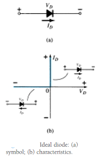
The ideal diode is a 2 pin electronic component with the symbolic representation and traits as shown in the following figures:
 |
|
Figure 1.1
|
In an ideal condition, a diode will pass current in the direction determined with the arrow in the
The properties of a perfect diode closely resembles a switch which is able to conduct
current in only a single direction.
In the explanation of the various aspects to follow, it is crucial that the various letter
When the polarity of the applied voltage is in line with that shown in above, the part of the characteristics that is to be observed in Fig. 1.1b is to the right of the vertical axis. In case a opposite
When the current through the diode contains the direction as suggested in Fig. 1.1a, the section of the characteristics to be looked at is over the horizontal axis, while a reversing in direction would demand the use of the attributes under the axis.
For most of the device attributes that come in this website, the ordinate (or “y” axis) stands out as the current axis, while the abscissa (or “x” axis) would be the voltage axis.
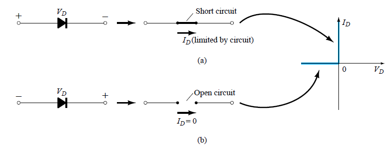
Among the essential parameters for the diode is the resistance in the point or area

where VF is the forward voltage across the diode and IF is the forward current through
The ideal diode, as a result, can be a short circuit for the region of conduction.
Look at the region of negatively placed voltage difference (3rd quadrant) of Fig. 1.1b,
 |
in which VR is reverse voltage across the diode and IR is reverse current through the diode.
The ideal diode, thus, is usually an open circuit in the region of non-conduction.
Doing a review, the situations represented in Fig. 1.2 can be applied
 |
|
Figure 1.2
|
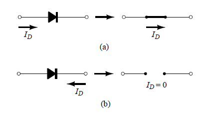
In most cases, it will be fairly easy to evaluate if a diode is in the region of conduction or non-conduction just by observing the direction of the current ID caused by a voltage.
For conventional polarity (opposite to that of electron flow), when the resulting diode current contains the same course as the arrow symbol of the diode, the diode is functioning on the conducting region as portrayed in Fig. 1.3a.
In case the current flow comes with the reverse direction, as indicated in Fig. 1.3b, the open circuit counterpart would be applicable.
 |
|
Figure 1.3
|
As pointed out previously, the main intent behind this segment is to present the characteristics
As we advance with the up coming several descriptions, make sure to preserve the following inquiries in mind:
How close does the forward or “on” resistance of a realistic diode compare
Will the reverse-bias resistance be adequately large to enable an open-circuit estimation?
1.3 SEMICONDUCTOR MATERIALS
The tag semiconductor on its own gives a tip as to its properties. The prefix semi is actually
typically given to a selection of ranges midway in between a pair of boundaries.
The phrase conductor is ascribed to just about any material that may help an ample
flow of charge any time a voltage source of a restricted degree is implemented over its terminals.
An insulator can be a material which offers an extremely low level of conductivity under
strain from an applied voltage supply.
A semiconductor, consequently, is often a material that features a conductivity grade anywhere
between the two extremes of an insulator and a conductor.
Inversely relevant to the conductivity of a substance is its resistance to the circulation of
charge, or current. In other words, the larger the conductivity amount, the lower the resistance
level.
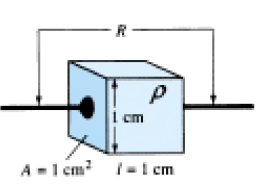
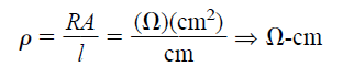
In tables, the phrase resistivity ( , Greek letter rho) is frequently applied when you compare
the resistance degrees of components. In metric units, the resistivity of a substance is
calculated in -cm or -m.
 |
|
Figure 1.4 |
The units of -cm are acquired from the replacement of the units for each expression of Fig. 1.4 into the below given equation (extracted from the fundamental resistance equation R = ?l / A
Actually, when the region of Fig. 1.4 is 1 cm2 and the length 1 cm, the value of the
resistance of the cube of Fig. 1.4 will be corresponding to the value of the resistivity of the
substance as confirmed below:
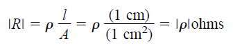
This fact can be beneficial to remember as we evaluate resistivity levels in the next conversations.
In Table 1.1, standard resistivity values are offered for 3 general groups of elements. Even though you could be aware of the electrical attributes of copper and mica from your earlier scientific studies, the characteristics of the semiconductor components of germanium (Ge) and silicon (Si) could possibly be fairly new.
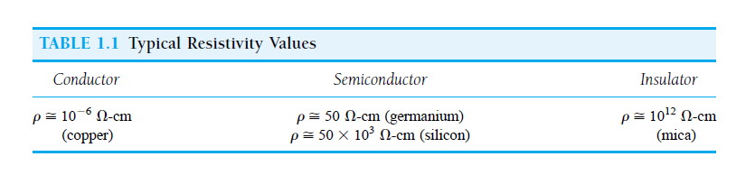
While you will discover in the chapters to follow, they may be definitely not the just 2 semiconductor elements. They may be, however, the two elements which have acquired the largest range of affinity for the expansion of semiconductor products.
Lately the move continues to be progressively toward silicon and away from germanium, yet germanium continues to be in moderate manufacturing range.
Observe in Table 1.1 the extreme range between the conductor and insulating components happens to be for the 1-cm length (1-cm2 area) of the substance. Eighteen areas split the placement of the decimal point for one number from the other. Ge and Si have obtained the interest they have for several motives.
One extremely important thought is the truth that they can be produced to a very good purity grade. In reality, latest advancements have minimized impurity degrees in the pure materials to a ratio of 1 in 10 billion (1 10,000,000,000). One may possibly question if these reduced impurity levels are actually needed.
They surely are when you take into account the inclusion of a single part impurity (of the proper type) for each million within a slice of silicon material can transform that substance from a somewhat bad conductor to a very good conductor of electricity.
We are naturally coping with completely new range of assessment ranges when we deal with the semiconductor medium.
Additional factors range from the proven fact that their qualities could be modified substantially with the implementation of heat or light which may be regarded as a crucial concern in the development of heat- and light dependent devices.
 |
|
Figure 1.5 |
A few of the distinctive features of Ge and Si mentioned above are because of their atomic structure. The atoms of each materials form a pretty precise pattern which is intermittent in nature (i.e., continuously repeats itself).
One full pattern is known as a crystal and the periodic set up of the atoms a lattice. For Ge and Si the crystal offers the 3D diamond framework of Fig. 1.5.
Any stuff made up of exclusively of reproducing crystal structures of the similar variety is named a single-crystal structure. For semiconductor elements of practical application in the field of electronics, this individual crystal characteristic is present, and, additionally, the periodicity of the composition is not going to alter appreciably with the inclusion of impurities during the doping process.
We will now analyze the construction of the atom on its own and observe how it could impact the electrical attributes of the substance. As you are mindful, the atom consists of 3 fundamental particles: the electron, the proton, and the neutron.
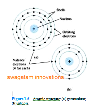
Within the atomic lattice, the neutrons and protons become the nucleus, while the electrons move close to the nucleus within a set orbit. The Bohr models of the two most frequently used semiconductors, germanium and silicon, are demonstrated in Fig. 1.6.
As pointed out in Fig. 1.6a, the germanium atom possesses 32 orbiting electrons, while silicon carries 14 orbiting electrons. In each scenario, you will find 4 electrons within the outermost (valence) shell.
The potential (ionization potential) needed to knock of any one of these 4 valence electrons is lower compared to for any other electron in the framework. In a pure germanium or silicon crystal these 4 valence electrons are usually strongly attached to 4 adjacent atoms, as displayed in Fig. 1.7 for silicon.
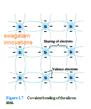
Despite the fact that the covalent bond can lead to a more powerful bond between the valence electrons and their parent atom, it is still likely for the valence electrons to soak up ample kinetic energy from natural factors to separate the covalent bond and move into the “free” status.
The word free explains that their movement is fairly sensitive to the subjected potential differences like influenced by voltage sources.
These natural factors consist of effects like light energy available as photons and heat energy from the atmospheric medium. At room temperature you will find roughly 1.5 x 10¹⁰ free carriers within a cubic centimeter of inbuilt silicon substance.
Innate or intrinsic substances are those semiconductors which were meticulously processed to minimize the impurities to a surprisingly low level, primarily as pure as can be produced by means of today's technology.
The free electrons inside the substance because of just natural reasons are known as intrinsic carriers. At an uniform temperature, intrinsic germanium substance could have roughly 2.5 x 10¹³ free carriers per cubic centimeter.
The proportion of the amount of carriers in germanium compared to that of silicon is higher than 103 and would signify that germanium is actually a better conductor in room temperature. This can be correct, however the two are still regarded as weak conductors in the intrinsic state. Observe in Table 1.1 the resistivity also varies with a ratio of approximately 1000:1, with silicon finding the bigger value. This must be the case, obviously, because resistivity and conductivity are oppositely related.
A rise in temperature of a semiconductor can lead to an amazing upsurge in the amount of free electrons within the material.
As the temperature goes up out of absolute zero (0 K), an growing amount of valence electrons absorb ample thermal energy to break up the covalent bond and add to the quantity of free carriers as explained before. This elevated number of carriers increases the conductivity index and results in a reduced resistance level.
Semiconductor materials like Ge and Si that exhibit a decrease in resistance value with rise in temperature are believed to possess a negative temperature coefficient.
You will likely remember that the resistance of the majority of conductors boosts with temperature.
The main reason for this is the proven fact that the numbers of carriers in a conductor will not rise appreciably with temperature, however their oscillatory pattern around a relatively static position is likely to make it progressively challenging for electrons to cross through. A rise in temperature thus produces a heightened resistance level and a positive temperature coefficient.
1.4 ENERGY LEVELS
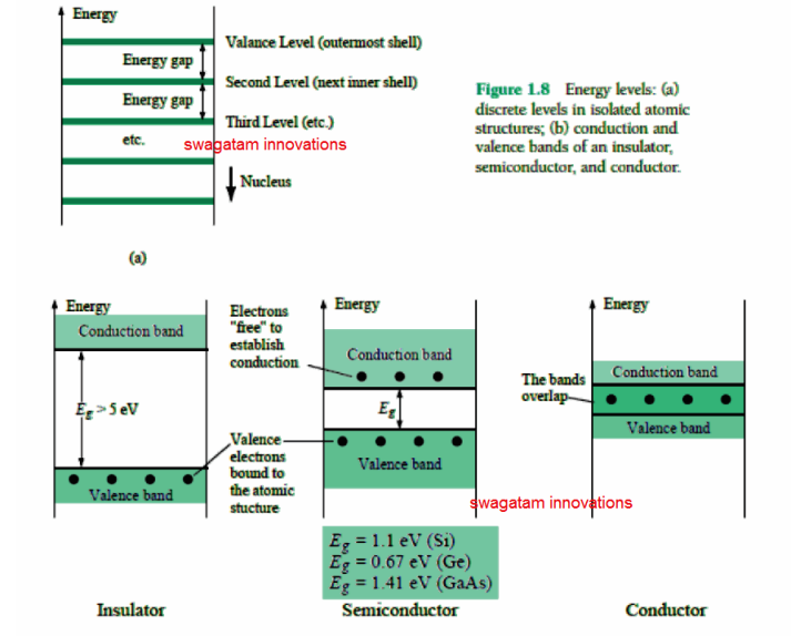
In the isolated atomic composition you will find individual energy levels linked to each orbiting electron, as demonstrated in Fig. 1.8a. Each content will, actually, possess its very own number of allowable energy levels for the electrons within the atomic framework.
The more faraway the electron from the nucleus, the greater the energy level, and any electron which has departed its parent atom carries a greater energy state compared to any electron inside the atomic composition.
as extracted from the determining equation for voltage V = W/Q. The charge Q happens to be the charge linked to a single electron.
Replacing the charge of an electron and a potential difference of 1 volt into Eq. (1.2) can lead to an energy level known as one electron volt. Given that energy can also be measured in joules and the charge of one electron 1.6 x 10⁻¹⁹ coulomb,
W = QV = (1.6 x 10⁻¹⁹ C)(1V)
1 eV = 1.6 x 10⁻¹⁹ J ---------------(1.3)
At 0 K or absolute zero ( 273.15°C), all the valence electrons of semiconductor elements end up getting locked within their outermost shell of the atom with levels of energy linked to the valence band of Fig. 1.8b. But, at room temperature (300 K, 25°C) numerous valence electrons attain adequate energy to abandon the valence band, get across the energy gap characterized by Eg in Fig. 1.8b and get into the conduction band.
For silicon Eg is 1.1 eV, for germanium 0.67 eV, and for gallium arsenide 1.41 eV. The undoubtedly lower Eg for germanium is liable for the enhanced quantity of carriers in that material than silicon at room temperature.
Observe for the insulator the energy gap is commonly 5 eV or higher, that significantly restricts the quantity of electrons going into the conduction band at normal temperature. The conductor has electrons in the conduction band even at 0 K. Pretty naturally, hence, at room temperature you will find ample free carriers to support huge stream of charge, or current.
We are going to discover in Section 1.5 that when particular impurities are put into the intrinsic semiconductor materials, energy states within the forbidden rings initiates causing a decrease in Eg for both semiconductor materials, consequently boosting carrier density within the conduction band at room temperature!
1.5 EXTRINSIC MATERIALS—
n- AND p-TYPE
The properties of semiconductor materials may be re-structured substantially through the supplement of several impurity atoms into the reasonably pure semiconductor material. These types of impurities, although are only introduced at probably 1 portion in 10 million, has the ability to modify the band structure adequately, transforming the electrical properties of the material completely.
A semiconductor content which has been afflicted by the doping process is known as an extrinsic material.
You will find a couple of extrinsic materials of outstanding significance to semiconductor device manufacturing: n-type and p-type. Each one are going to be explained in certain depth in the next paragraphs.
n-Type Material
Both n- and p-type materials are created with the addition of a predetermined quantity of impurity atoms into a germanium or silicon base. The n-type is produced by adding those impurities that contain 5 valence electrons (pentavalent), for example antimony, arsenic, and phosphorus. The result of such impurity elements is pointed out in
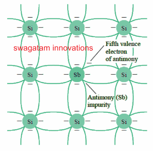
Remember that the 4 covalent bonds continue to be present. There exists, however, one particular more 5th electron because of the impurity atom, that is dissociated with any specific covalent bond. This leftover electron, freely bonded to its parent (antimony) atom, is fairly liberal to move inside the freshly created n-type material. Because the injected impurity atom has contributed a rather “free” electron to the structure:
Diffused impurities having 5 valence electrons are classified as donor atoms.
You should understand that despite a good number of “free” carriers are established in the n-type material, it is even now electrically neutral because ultimately the quantity of positively charged protons within the nuclei continues to be same as the number of “free” carriers and moving around the negatively charged electrons in the composition.
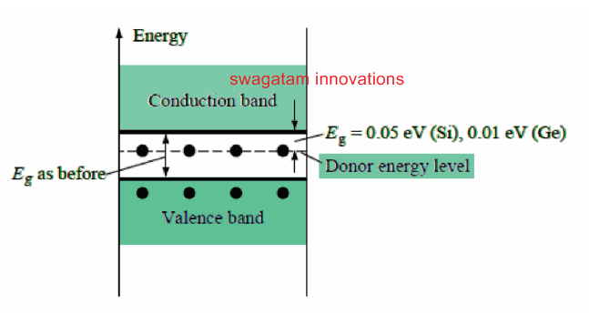
The result of this doping method on the relative conductivity can be appropriately detailed by using the energy-band diagram of Fig. 1.10. See that a discrete energy level (referred to as donor level) shows up in the forbidden orbit having an Eg substantially lower than that of the intrinsic material.
These “free” electrons as a result of added impurity rest at this energy level and quite easily absorb an adequate amount of thermal energy to shift into the conduction band in ambient temperature.
In this way at room temperature, we see a large number of carriers (electrons) in the conduction level and the conductivity of the substance goes up enormously. At room temperature in an intrinsic Si material you can find around one free electron for each 1012 atoms (1 to 109 for Ge).
If our doping level had been 1 in 10 million (107), the ratio (1012/107) would likely signify that the carrier concentration has grown by a proportion of 100,000 :1.
The p-type material is created by doping a pure germanium or silicon crystal with impurity atoms obtaining 3 valence electrons. The things normally employed for this operation are boron, gallium, and indium. The influence of one of these factors, boron, over a base of silicon is shown below.
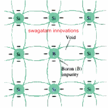
The diffused impurities with 3 valence electrons are known as acceptor atoms.
The resultant p-type material will be electrically neutral, for the similar factors explained for the n-type material.
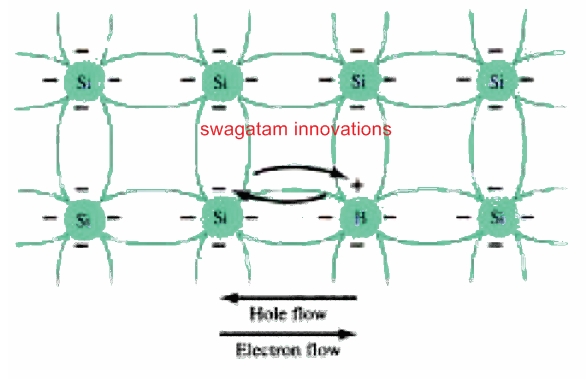
Electron versus Hole Flow
The impact of the hole upon conduction is presented in Fig. 1.12. In case a valence electron obtains ample kinetic energy to split its covalent bond and scatters in the void developed by a hole, then a vacancy, or hole, shall be produced in the covalent bond that discharged the electron.
Therefore, you find a exchange of holes to the left and electrons to the right, as demonstrated in Fig. 1.12. The direction to be employed in this text is the one about conventional flow, that is shown by the direction of hole movement.
Majority and Minority Carriers
In the intrinsic condition, the amount of free electrons in Ge or Si is only due to those handful of electrons in the valence band which have obtained adequate energy through heat or light sources to split the covalent bond or to the small amount of impurities which could not be eliminated.
The vacancies abandoned in the covalent bonding composition symbolize our highly restricted source of holes. In an n-type material, the amount of holes remain hugely unchanged from this intrinsic level. The net outcome, thus, is that the volume of electrons much exceeds the amount of holes. Therefore:
In an n-type material (Fig. 1.13a) the electron is known as the majority carrier and the hole the minority carrier.
For the p-type material the quantity of holes much exceeds the amount of electrons, as shown in Fig. 1.13b. Hence:
In a p-type material the hole turns out to be the majority carrier and the electron the minority carrier.
When the 5th electron of a donor atom departs the parent atom, the left over atom obtains a net positive charge: therefore the positive sign in the donor-ion manifestation. For very much the same reasons, the negative sign seems in the acceptor ion.
The n- and p-type materials symbolize the fundamental foundation of semiconductor equipment. We are going to come across in the next segment how the “joining” of a single n-type material with a p-type material constitutes a semiconductor component of substantial value in electronic circuits.

1.6 SEMICONDUCTOR DIODE
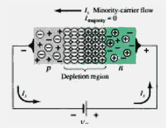
In Section 1.5 both the n- and p-type materials had been discussed. The semiconductor diode is established simply by getting these components jointly (made of the same base-Ge or Si), as demonstrated in Fig. 1.14, through methods that will be explained in Chapter 20.
The moment both materials are “joined” the electrons and holes around the junction merge, creating deficiency of carriers in the area close to the junction.
This region of exposed positive and negative ions is known as the depletion area as a result of depletion of carriers in this area.
Because the diode happens to be a two-terminal unit, the supply of voltage across its leads produces 3 possibilities: no bias (VD = 0 V), forward bias (VD > 0 V), and reverse bias (VD < 0 V).
Each can be a situation that may give rise to a reaction that the user should understand fully to ensure an effective use of the device.
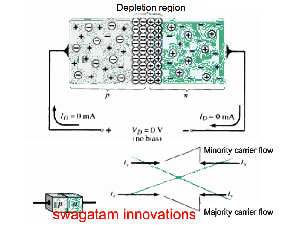
No Applied Bias (VD = 0 V)
In the no-bias (zero voltage) situations, any minority carriers (holes) within the n-type material which happen to be within the depletion area will move straight into the p-type material.
The nearer the minority carrier would be to the junction, the higher the attraction for the layer of negative ions and the less the opposition of the positive ions in the depletion region of the n-type material.
For using in future discussions we need to imagine all the minority carriers of the n-type material which locate themselves in the depletion region because of their arbitrary motion may cross straight into the p-type material.
Identical discourse could be ascribed to the minority carriers (electrons) of the p-type material. This particular carrier flow can be seen in Fig. 1.14 for the minority carriers of each material.
The majority carriers (electrons) of the n-type material need to defeat the pulling forces of the layer of positive ions in the n-type material and the defenses of negative ions in the p-type material in order to jump over to the area outside of the depletion region of the p-type material.
Nonetheless, the amount of majority carriers happens to be so huge in the n-type material that there may be inevitably hardly any majority carriers having enough kinetic energy to cross over the depletion region into the p-type material.
Yet again, the identical type of definition could be used on the majority carriers (holes) of the p-type material. The resulting movement because of the majority carriers can also be seen in Fig. 1.14.
An in depth study of Fig. 1.14 may show that the relative dimensions of the flow vectors are in a way that the net flow in either route is zero.
This particular termination of vectors can be seen in the form of crossed lines. The span of the vector symbolizing hole flow is sketched longer than that for electron flow to show that the degree of each does not need to be identical for canceling and that the doping levels for each material may end up in an ununiform carrier flow of holes and electrons. Hence we can summarize:
In the absence of a biasing voltage, the net flow of charge in a given direction for a semiconductor diode will be zero.
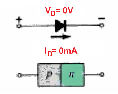
The symbolic representation for a diode is repeated in Fig. 1.15 using the related n- and p-type regions. Observe that the arrow direction is connected with the p-type component and the straight bar with the n-type region. As pointed out, for VD 0 V, the current flowing in any direction will be 0 mA.
Reverse-Bias Condition (VD < 0 V)
If an external voltage difference V volts is employed across the p-n junction in a way that the positive terminal is attached to the n-type material and the negative terminal is linked to the p-type material as shown in Fig. 1.16, the volume of uncovered positive ions within the depletion region of the n-type material increases because of the huge amount of “free” electrons driven towards the positive potential of the connected voltage. Similarly, the volume of exposed negative ions increases in the p-type material.
The overall impact, thus, is a broadening of the depletion region. This broadening of the depletion region creates sufficiently large barrier for most carriers to overcome, effectively lowering the majority carrier movement to zero as demonstrated in Fig. 1.16.
The current that is present within reverse bias situations is known as the reverse saturation current and is symbolized by Is.
The reverse saturation current is rarely over some microamperes excluding high-power devices. Actually, nowadays its level is usually within nanoamperes for silicon devices and in the lower microampere range for germanium.
The term saturation originates from due to the reason that it extends to its highest level rapidly and doesn't alter much even with an escalation in the reverse-bias voltage, as demonstrated on the diode characteristics of Fig. 1.19 for VD 0 V.
The reverse-biased situations are represented in Fig. 1.17 for the diode symbol and p-n junction. Be aware, specifically, that the direction of Is is in opposition to the arrow of the symbol.
Observe likewise that the negative potential is attached to the p-type material and the positive potential to the n-type material the difference in underlined letters for each location indicating a reverse-bias situation.
Forward-Bias Condition (VD > 0 V)
A semiconductor diode is forward-biased whenever the association p-type and positive and n-type and negative is created

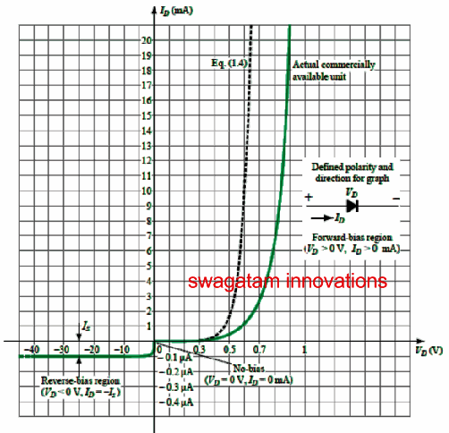

Be aware in Fig. 1.19 that the units available in marketplaces offer characteristics which are displaced to the right by a several tenths of a volt.
The main reason for this is the internal “body” resistance and external “contact” resistance of a diode.
Each plays a role in an extra voltage with the same current level as decided by Ohm’s law (V = IR). Over time, as manufacturing techniques develop, this difference may minimize and the real characteristics could closely match those of Eq. (1.4).
It may be essential to be mindful of the change in scale for the vertical and horizontal axis. For positive values of ID the scale is in milliamperes and the current scale under the axis is in microamperes (or even nanoamperes). For VD the scale for positive values is in tenths of volts and for negative values the scale is in tens of volts.
At first, Eq. (1.4) does seem relatively complicated and might establish an unnecessary worry that it may be reproduced for all the subsequent diode applications. Thankfully, however, several approximations will probably be done in a later segment which will avoid the necessity to apply Eq. (1.4) and provide a remedy with least statistical complexities.
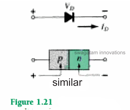
Before ending this topic regarding forward-bias condition the situations for conduction (the “on” state) are repeated in Fig. 1.21 using the recommended biasing polarities and the resulting direction of majority-carrier flow. Observe specifically the way the path of conduction complements the arrow in the image (as suggested for an ideal diode).
Although the scale of Fig. 1.19 is in 10s of volts in the negative region, there exists a position where the application of too negative a voltage can lead to an intense change
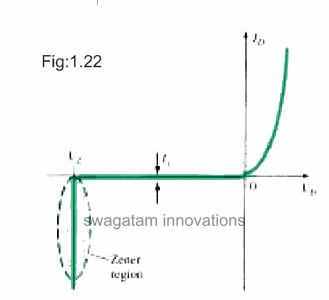
As the voltage over the diode rises in the reverse-bias region, the acceleration of the minority carriers accountable for the reverse saturation current Is likewise increases. Sooner or later, their acceleration and associated kinetic energy (WK = 1/2 mv2) is going to be enough to discharge supplemental carriers via collisions with normally stable atomic structures. Meaning, an ionization course of action may effect whereby valence electrons absorb adequate energy to abandon the parent atom. All these supplemental carriers may then help the ionization approach until an increased avalanche current is determined and the avalanche breakdown area established.
The avalanche region (VZ) could be carried nearer to the vertical axis by raising the doping levels in the p- and n-type materials.
However, as VZ lowers to minimal levels, for example 5V, a different process, called Zener breakdown, adds to the sharp enhancements on the characteristic. It happens since there is a powerful electric field around the junction having the ability to break up the bonding forces within the atom and “create” carriers.
Although the Zener breakdown mechanism is a substantial contributor only at smaller degrees of VZ, this distinct change in the attribute at any level is known as the Zener region and diodes utilizing this distinctive part of the characteristic of a p-n junction these are known as Zener diodes. They are detailed in depth in Section 1.14.
The Zener region of the semiconductor diode detailed has to be ignored if the reaction of a system is not to be fully changed by the sharp change in characteristics in this reverse-voltage area.
The highest reverse-bias potential which can be employed prior to entering the Zener region is known as the peak inverse voltage (simply known as the PIV rating) or the peak reverse voltage (designated by PRV rating).
If an application needs a PIV rating higher than that of a single unit, several diodes having the identical specs could be hooked up in series. Diodes may also be joined in parallel to boost the current carrying ability.
Silicon versus Germanium
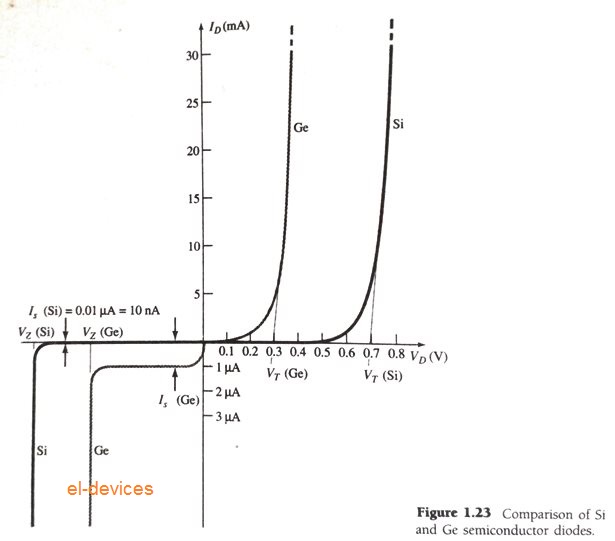
VT = 0.3 (Ge)
Temperature Effects
Temperature may have a noticeable impact on the properties of a silicon semiconductor diode as may be observed by a standard silicon diode in Fig. 1.24. It is often identified experimentally that:
The reverse saturation current Is happens to be practically twice in value for each 10°C rise in temperature.
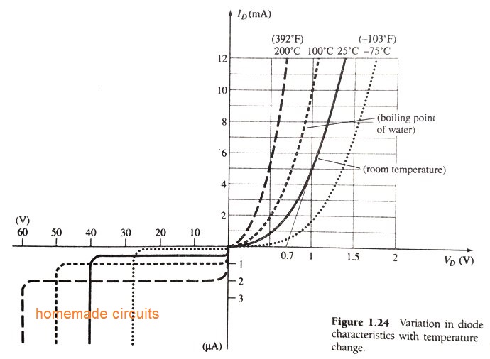
The growing levels of Is with temperature account for the reduced levels of voltage limits, as demonstrated in Fig. 1.24.
Simply raise the level of Is in Eq. (1.4) and observe the sooner rise in diode current. Needless to say, the level of TK will also be escalating in the same equation, however the growing amount of Is may begin controlling the smaller change in TK.
As the temperature raises, the forward characteristics are in fact turning into more “ideal,” however we may discover when we overview the specifications datasheets that temperatures above the standard working range may have an extremely adverse influence on the diode’s optimum power and current ranges.
In the reverse-bias region the breakdown voltage is raising with temperature, but observe the unfavorable upsurge in reverse saturation current.
1.7 RESISTANCE LEVELS
As the operational point of a diode shifts from a single region to a new, the resistance of the diode will likely alter because of the non-linear style of the characteristic curve.
It'll be proven over the following several paragraphs that the form of applied voltage or signal may determine the resistance level of interest.
3 diverse ranges may be witnessed in this segment which may be used again and again as we analyze additional devices. It is for that reason extremely important that their evaluation be clearly grasped.
DC or Static Resistance
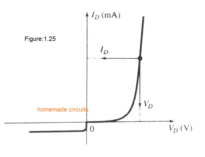
The usage of a dc voltage into a circuit comprising a semiconductor diode may lead to an operational stage on the characteristic curve that won't alter in response to time. The diode resistance at the operating point can be determined simply by calculating the communicating levels of VD and ID as proven in Fig. 1.25 and by implementing the below formula:
RD = VD / ID -------------(1.5)
The dc resistance values at the knee and under knee level is going to be higher than the resistance values acquired for the vertically increasing portion of the characteristics.
The resistance values in the reverse-bias area will obviously be extremely high. Due to the fact ohmmeters usually require a fairly constant-current supply, the resistance established is going to be at a predetermined current level (normally, some milliamperes).
AC or Dynamic Resistance
It is apparent from Eq. 1.5 and Example 1.1 that the dc resistance of a diode is not dependent on the appearance of the characteristic in the area around the point of interest.
In case a sinusoidal instead of dc input is utilized, the scenario changes entirely. The changing input will shift the instantaneous operating level along a region of the characteristics and therefore identifies a particular alteration in current and voltage as displayed in Fig. 1.27.
With a non varying constant signal input, the point of operation would be the Q-point as can be seen on Fig. 1.27 established through the applied dc levels. The naming Q-point comes from the word quiescent, meaning “constant or unchanging.”
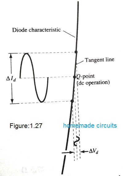
A straight line drawn tangent to the curve via the Q-point as indicated in Fig. 1.28 establishes a specific alteration in voltage and current which you can use to ascertain the ac or dynamic resistance in this area of the diode characteristics.
An attempt must be made to maintain the change in voltage and current as little as you can, and equidistant to both side of the Q-point.
As an equation:
rd = ?Vd / ?Id
where ? denotes the restricted change in the quantity
This implies, typically, the lower the Q-point of operation (that is for smaller current or lower voltage) the bigger will be the ac resistance.
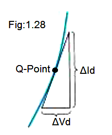
We have observed the dynamic resistance through graph representation, however you will find a simpler definition in differential calculus which will say:
The derivative of a function at a point is equal to the slope of the tangent line drawn at that point.
Equation (1.6), as outlined by Fig. 1.28, is, as a result, in essence finding the derivative of the function in the Q-point of operation.
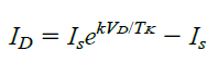
Finding the derivative of the standard equation (1.4) for the semiconductor diode based on the forward biasing, and subsequently inverting the result, produces an equation for the dynamic or ac resistance in that region. Meaning, considering the derivative of Eq. (1.4) with reference to the biasing voltage may produce:
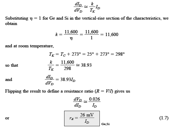
The importance of Eq. (1.7) has to be clearly comprehended. This signifies that the dynamic resistance can be obtained basically by replacing the quiescent value of the diode current into the equation.
You don't need to get hold of the characteristics or stress about drawing tangent lines as identified by Eq. (1.6). It is crucial to remember, however, that Eq. (1.7) is precise specifically for values of ID in the vertical-rise area of the curve.
For lower values of ID, 2 (silicon) and the value of rd acquired should be multiplied with a factor of 2. For lesser values of ID under the knee of the curve, Eq. (1.7) results in being incorrect.
All the resistance quantities established so far happen to be characterized by the p-n junction and don't have the resistance of the semiconductor material on its own (identified as body resistance) and the resistance created by the networking between the semiconductor content and the outside metal conductor (referred to as contact resistance).
These types of supplemental resistance quantities could be incorporated into Eq. (1.7) with the addition of resistance designated by rB as appearing in the following Eq. (1.8).
The resistance r 'd, therefore, includes the dynamic resistance defined by Eq. 1.7 and the resistance rB currently introduced .
In fact, identifying rd to some higher level of precision from a characteristic curve implementing Eq. (1.6) can be a challenging approach at best and the outcomes must be dealt with a grain of salt.
At lower levels of diode current the element rB is generally modest enough in comparison to rd to allow overlooking its effect on the ac diode resistance.
At higher degrees of current the level of rB may well approach that of r'd, however considering that there will often be additional resistive aspects of a much bigger dimensions in series with the diode we are going to presume in this book that the AC resistance is established exclusively by r'd and the influence of rB will likely be ignored unless otherwise taken into consideration.
Scientific enhancements of recent years claim that the degree of rB may carry on and decline in value and in the end turn into an element that could undoubtedly be ignored compared to rd.
The topic above has focused solely on the forward-bias area. In the reverse-bias region we are going to imagine the change in current over the Is range is nil from 0V to the Zener area and the resulting ac resistance utilizing Eq. (1.6) is adequately high to enable the open-circuit estimation.
Average AC Resistance
In case the input signal is adequately big to generate a wide swing like as pointed out in Fig. 1.30, the resistance linked to the device with this area is known as the average ac resistance.
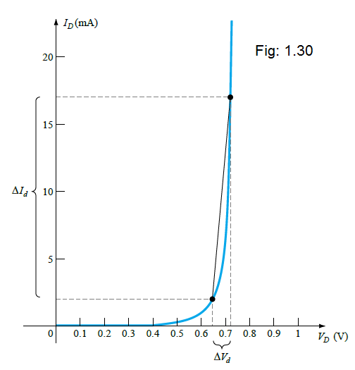
The average ac resistance is, by definition, the resistance decided by a straight line sketched across the two intersections established by the highest and lowest values of input voltage. As an equation form (observe Fig. 1.30),
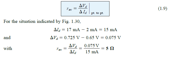
In case the AC resistance (rd) were identified at ID = 2 mA its value would be greater than 5? , and when established at 17 mA it would be less.
In middle of the ac resistance would cause the changeover from the higher value at 2 mA to the lower value at 17 mA.
Equation (1.9) has identified a value which is regarded as the average of the AC levels from 2 to 17 mA.
The fact that one resistance level may be used for this kind of a broad range of the characteristics will prove pretty useful in the definition of comparable circuits for a diode within a later section.
Much like the dc and ac resistance levels, the lower the condition of currents accustomed to decide the average resistance the larger the resistance level.
In the next chapter we will learn about Diode Equivalent Circuits