

The proposed low dropout regulator circuit is built using ordinary bipolar transistors, and can be effectively used for getting an output virtually zero drop. Meaning suppose if the circuit is intended for getting 5 V regulated from a 5 V to 7 V supply it would give a stabilized fixed output which will be almost equal to a constant 5 V.
In regulator power supply circuits where the input and output voltages aren’t equal, the application of integrated 3-pin voltage regulators like7805, 7812, 7824 etc are not encouraged.
Disadvantage of Standard 3 pin Regulators
The drawback with most of the 3-pin regulators is that they need an input voltage which must be 3 V more than the voltage at the output.
In applications where input and output voltages are nearly identical, then it is better to use a customized low dropout regulator circuit using discrete components as explained below.
In a typical emitter circuit, the series transistor is connected so that there is a lower output voltage than the input voltage but only through the saturation voltage of the transistor. Nevertheless, it will be challenging to deliver short-circuit protection.
Figure 1 represents the series transistor gets its base current from T2 which combines itself with T1 to form a differential amplifier.

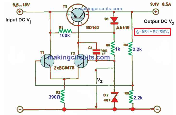
This setup makes sure that the D2’s cathode and the junction of voltage divider R4-R5 have equal voltage. The main part for the circuit is T3 which occupies definite current amplification.
However, T2 can only supply the amount of base current that R2 permits. The differential voltage across R2 has a maximum value of the Zener diode sans the base-emitter voltage, VBE, of T2, which is around 4 V. The maximum current that passes R2 is more or less 11 mA.
Output Current Range
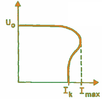
When we assume the T3 has a current amplification capacity of 50, the maximum output current would be around 0.55 A. Let’s say a stronger current is drawn, then there will be a drop in the output voltage. Say the drop in voltage is lower than D2’s voltage, the potential difference across R2 will also drop.
As a result, the output current will react as depicted in Figure 2 which describes its fold-back properties. Evidently, we have proof that the series transistor is safeguarded against high, short-circuit currents.

Diode D1 and resistor R1 deliver a soft launch because the voltage across the diode is zero at switch-on mainly due to its connection to the regulator’s output. The circuit may oscillate because of high gain but this can be stabilised when capacitor C1 is added.
How to Select the LDO Output Voltage
The output voltage level, V0, of this low dropout voltage regulator circuit is free to select but you have to make sure it stays within the range of series transistor and D2, R3 and R4. The formula below is used to determine the output voltage level:
V0 = Vz (R5 + R4 / R5)
It is important to equate resistor R2 with the actual current amplification of the transistor. It is noted that a properly cooled BD140 has a maximum dissipation of 5 W.
Moreover, if a noise-free output is needed, an additional 10 µF electrolytic capacitor must be attached in parallel to D2. All this allows a soft start for the circuit with practically no output for about 0.2 s after it is switched on.