Simple transistor tester circuit is quite easy and low cost circuit, is just not built to calculate any transistor efficiency figures, however is designed to get fast testing to signify if the test device is well designed.
The standard technique of examining a transistor would be to initially link a supply to its emitter and collector terminals and be sure that no considerable current flows.
In case the base terminal is then provided a small forward bias, this can be increased by means of a large collector emitter current.
Simple transistor tester circuit is dependent on a CMOS quad 2 input NAND or NOR gate IC. Both form is appropriate as each gate possesses its two inputs attached with each other in order that it functions as an inverter.
The first two inverters are employed together with R1 and C1 like a standard CMOS oscillator working at a frequency of a few hundred Hz. The other two inverters are linked in parallel, and fed through the output of the oscillator to make sure they supply a subservient output.
This means that, one output will probably be positive and also the other will probably be negative apart from through the short intervals once the outputs change state.
The collector and emitter of the transistor tend to be provided through the outputs via D1 and D2, plus the base is given from one output via R2.
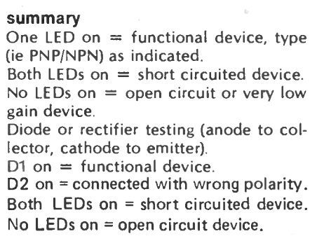
Once we imagine an NPN device has been tested, when gate 2 output is positive as well as other output is negative, the transistor will never be ahead biased through R2 (it will likely be reverse biased actually) and it need to cross no considerable collector current.


In case it is a short circuit device will not pass this sort of current, this can go through D2 that may illuminate and signify the wrong doing.
Once the outputs happen to be in the opposite states, the transistor will probably be forward biased through R2 and really should perform intensely, leading to D1 to pass a current and illuminate.
Failure of D1 to come on signifies an open circuit or minimal gain device.
PNP devices work with the opposite polarity, and thus when testing these types of it really is D2 which should turn on, and D1 which will continue to be off.

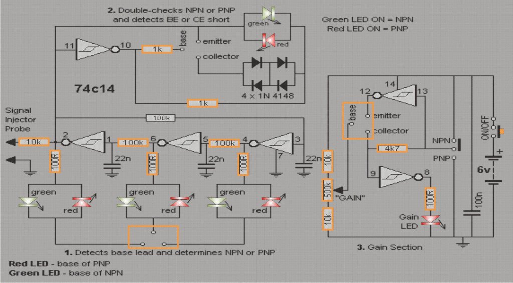
Another Transistor Tester Design
This simple transistor tester circuit can be used to test the polarity of BJT transistors and verify whether it is an NPN or PNP.
How to Test
Test Process: Position the transistor to the three circuit terminals of Circuit 1 (located either below of left of the terminal).
Once pointed, the red LED can then identify the PNP transistor base.
This process will lead to the emission of a green LED, which points to the base of the NPN conductor.
Test Process 2: Now that you are aware of the transistor type and the base lead, simply position the transistor in the top circuit (Test 2).
As you properly place the collector, the emitter works perfectly.
However, there may be a chance to swipe leads in case if it fails to work.
If the red and green LED works it proves the transistor is functional correctly.
Test Process 3: The transistor is now ready to be placed in the GAIN SECTION.
Select either NPN or PNP. As you select, simply turn on the pot and keep it turned as long as the LED is illuminated.
However, as a matter of practice be sure to check the value of the gain mentioned in the PCB.
The probe located at the end of the board helps to create square wave.
Furthermore, this simple transistor tester probe is also efficient to testing audio of any sorts.