

Long back, the important and significant element of an electronic device used to be a vacuum tube; it is an electron tube accustomed to regulate electric current.
The vacuum tubes worked well however they were cumbersome, demanded greater running voltages, higher energy usage, delivered reduced performance and cathode electron-emitting resources were consumed in operation.
Therefore, resulting in the generation of heat which affected the life span of the tube per se. In order to rectify these types of issues, John Bardeen, Walter Brattain and William Shockley together developed a transistor at Bell Labs back in of 1947.
The brand new product must have been a a lot more sophisticated way to get over most of the basic restrictions of vacuum tubes.
Transistor is a semiconductor device that can both conduct and insulate. A transistor can easily work as a switch and also like an amplifier. It transforms audio waves into digital waves using resistors, for controlling electronic current. Transistors possess extended life, are more compact in size, can run on reduced voltage supplies for better safety and does not depend on filament current.
The 1st transistor was manufactured with germanium. A transistor works with exactly the same principle as a vacuum tube triode, but utilizing semiconductor junctions as opposed to hot electrodes in a vacuum chamber. It is the essential foundation of modern electronics and observed everywhere contemporary electronic systems.
Transistor Basics:
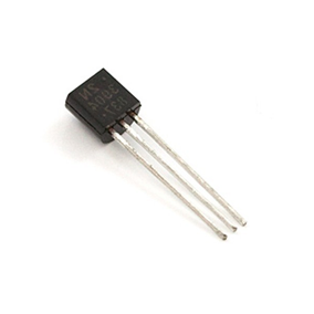
A transistor is a 3 pin unit. Namely,
Base: This is in charge of triggering the transistor.
Collector: This is the positive pin.
Emitter: This is actually the ground pin with respect to collector and base.
The fundamental concept behind a transistor is that it enables you to regulate the movement of current via one channel by adjusting the strength of a smaller current flowing via a subsequent channel.
Types of Transistors:
You will find two different types of transistors in currently; they may be bipolar junction transistor (BJT), field effect transistors (FET). A tiny current is moving between the base and the emitter; base terminal can easily regulate a bigger current circulation between the collector and the emitter pins. For any field-effect transistor, it also contains the 3 leads, they may be gate, source, and drain, and a voltage on the gate can easily regulate a current between source and drain.
The straightforward drawings of BJT and FET are demonstrated in figure below:


Basically, transistors are available in a range various sizes and cuts. A very important factor most of these transistors share is they all 3 pinouts.
Bipolar Junction Transistor:
A Bipolar Junction Transistor (BJT) provides 3 pins attached to 3 doped semiconductor areas. It is designed with two styles, P-N-P and N-P-N.
P-N-P transistor, comprising a layer of N-doped semiconductor between 2 levels of P-doped substance. The base current passing in the collector is increased at its output.
This is the moment when the PNP transistor is SWITCHED ON when its base is switched at low compared to the emitter. The arrows of PNP transistor symbolic representation shows the direction of current stream when the unit is in forward active mode.


N-P-N transistor containing a covering of P-doped semiconductor between two layers of N-doped material. By amplifying current at the base, we can have high collector and emitter currents.
This is the moement when NPN transistor is CONDUCTING AND IS ON when its base is drawn low compared to the emitter. As soon as the transistor is in CONDUCTING status, current flow is within collector and emitter of the transistor.
Depending on minority carriers in P-type region the electrons shifting through emitter to collector. It enables the higher current and speedier functioning; due to this reason the majority of bipolar transistors applied today are NPN.


Field Effect Transistor (FET):
The field-effect transistor is really a unipolar transistor, N-channel FET or P-channel FET are applied for conduction. The 3 leads of FET are source, gate and drain.
The basic n-channel and p-channel FET’s are demonstrated above. For the n-channel FET, the device is fabricated from n-type material. Across the source and drain N-type material works as a resistor.
This transistor manages the positive and negative carriers with regard to holes or electrons. FET channel is created by relocating of positive and negative charge carriers. The channel of FET is essentially made by silicon.
You will find many types of FET’s, MOSFET, JFET and etc. The usage of FET’s have been in low noise amplifier, buffer amplifier and analog switch.
Bipolar Junction Transistor Biasing


Transistors are the most significant semiconductor active equipment necessary for just about all circuits. These are applied as digital switches, audio receivers etc in circuits.
Transistors could be NPN, PNP, FET, JFET etc that have various capabilities in electronic circuits. For the correct functioning of the circuit, it is important to bias the transistor through resistor networking. Operating point is the level on the output attributes that displays the Collector-Emitter voltage and the Collector current without any input signal.
The Operating point is additionally referred to as the Bias point or Q-Point (Quiescent point).
Biasing is known to provide resistors, capacitors or supply voltage etc to offer appropriate working qualities of the transistors. DC biasing can be used to get DC collector current at a specific collector voltage.
The level of this voltage and current are portrayed through Q-Point. In a transistor amplifier settings, the IC (max) is the optimum current that may move across the transistor and VCE (max) is the highest voltage utilized throughout the device. To operate the transistor like an amplifier, a load resistor RC should be attached to the collector.
Biasing establishes the DC operating voltage and current to the appropriate degree in order that the AC input signal could be effectively amplified by the transistor. The right biasing level is approximately the fully ON or fully OFF conditions of the transistor.
This core point is the Q-Point and when the transistor is correctly biased, the Q-point may be the key working point of the transistor. This can help the output current to boost and reduce as the input signal sways with the full cycle.
With regard to setting the right Q-Point of the transistor, a collector resistor is employed to fix the collector current to a consistent and stable value with no signal in the base.
This stable DC operating point fixed through the value of the supply voltage and the value of the base biasing resistor. Base bias resistors are employed in all the 3 transistor configuration settings like common base, common collector and Common emitter configurations.


Modes of biasing:
The below given are the various methods of transistor base biasing:
1. Current biasing:
As demonstrated in the Fig.1, 2 resistors RC and RB are accustomed to fix the base bias. These resistors create the primary operating region of the transistor through a fixed current bias.
The transistor forward biases having a positive base bias voltage by means of RB. The forward base-Emitter voltage drop is 0.7 volts. Which means current via RB is IB = (Vcc - VBE ) / IB
2. Feedback biasing:
Fig.2 exhibits the transistor biasing through a feedback resistor. The base bias is acquired through the collector voltage. The collector feedback makes certain that the transistor is constantly biased in the productive region.
Once the collector current raises, the voltage in the collector declines. This decreases the base drive that consequently decreases the collector current. This feedback setup is perfect for transistor amplifier styles.
3. Double Feedback Biasing:
Fig.3 exhibits the way the biasing is accomplished through dual feedback resistors.
By making use of 2 resistors RB1 and RB2 boosts the stability based on the disparities in Beta by raising the current flow via the base bias resistors. Within this settings, the current in RB1 is the same as 10 % of the collector current.
4. Voltage Dividing Biasing:
Fig.4 exhibits the Voltage divider biasing that has a couple of resistors RB1 and RB2, attached to the base of the transistor developing a voltage divider network. The transistor gets biased through the voltage drop throughout RB2. This type of biasing setup can be used extensively in amplifier circuits.
5. Double Base Biasing:
Fig.5 displays a double feedback for stabilization. It makes use of both Emitter and Collector base feedback to enhance the stability by means of manipulating the collector current. Resistor values must be decided on in order to establish the voltage drop over the Emitter resistor 10% of the supply voltage and the current via RB1, 10% of the collector current.
Advantages of Transistor:
Scaled-down mechanical sensitivity.
Less expensive and more compact in size, particularly in small-signal circuits.
Lower operating voltages for better protection, cut costs and firmer clearances.
Incredibly durability.
Absolutely no power consumption by way of a cathode heater.
Rapid switching.
It may support the appearance of complementary-symmetry circuits, something extremely hard with vacuum tubes. For those who have any questions with this subject or on the electrical and electronic projects leave the comments below.