

The MC14541B (or 4541) is a low cost IC that occupies a CMOS timer consisting of a 16-stage binary counter, an internal RC-oscillator circuit and an automatic power-up reset circuit, and a choice of output logic.
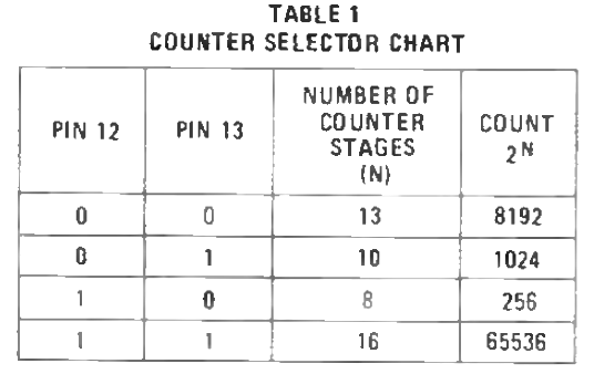
The 16-stage counter divides the oscillator frequency into four ever ready outputs of 28, 210, 213 and 216. The circuit sums 256 clock pulses for the least duration (28) and 65536 pulses for the longest interval (216). You can see the counting from the truth table shown in Figure 1.

By choosing the oscillator’s frequency and the amount of counter stages, the interval can be configured to just to any length you want.
Using the 14541
An easy universal programmable timer circuit is displayed in Figure 2 below.

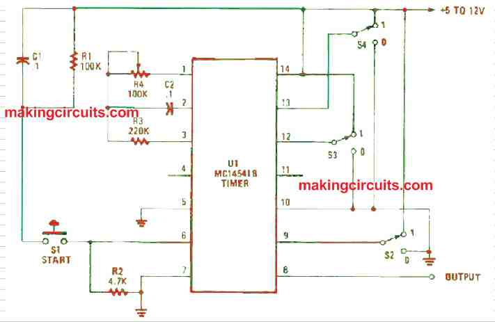
Once pin 5 of U1 is attached to a logic low (ground in our terms), the counter circuit gets set automatically the moment power is applied. The master reset which situates at pin 6 needs a positive pulse to reset the internal counters and commence the timing operation.
Pin 9 actuates the timer’s output mode. When you connect pin 9 to ground, it retains the timer’s output voltage (pin 8) at ground potential until the timing cycle is finished. After that, it switches to positive.
If you connect pin 9 to the V+ supply rail, the opposite output conditions occur where the output stays high until the timing cycle is finished and then it goes to low. The whole timing mode selection is facilitated through switch S2.
The timer’s whole count determines the positions of S3 and S4. Once S3 is in position 1 and S4 in position 0, the counter will sum up to 256 before a timeout. If you match the states of S3 and S4 to the truth table as described in Figure 1, you will be able to set to the needed count.
The internal oscillator is configured to the desired frequency with component values set by the formula f = 1/(2.3 x R4 x C2). Always make sure the value of R3 must be about twice the value of R4. One more thing you should verify is that R4 is always in Megaohms whereas C2’s capacitance must be in the range of microfarads.
Based on an example, the computed value was found to be 43.4 Hz, but our frequency counter measured 41 Hz, which is relatively close. As pin 10, the mode control, is attached to ground like in Figure 2, the timer functions in a single-cycle mode.
But, when pin 10 is linked to V+, the mode switches to recycling condition that makes the timing cycle to repeat continuously as long as there is power to the circuit.
To allow acquiring an accurate time delay, potentiometer R4 is used. After the needed resistor value is found, R4 can be swapped with a fixed 1% unit, or let it be until it can be changed later. The whole circuit can be reset by pressing switch S1.
MC14536 Programmable timer
The second universal programmable timer circuit in our experiment is constructed around an MC14536B programmable timer.
This IC has a 24-stage binary ripple counter with 16 stages within the unit that are selectable by a 4-bit binary code. Also, the timer comes with an in-built RC oscillator which is identical to the previous circuit.
This timer has a monostable-multivibrator output too. You can set almost any timing interval by choosing the clock frequency and the right counter stage for the wanted interval.
Most of the U1’s options are selectable through separate switches as shown in the timer circuit in figure 3.

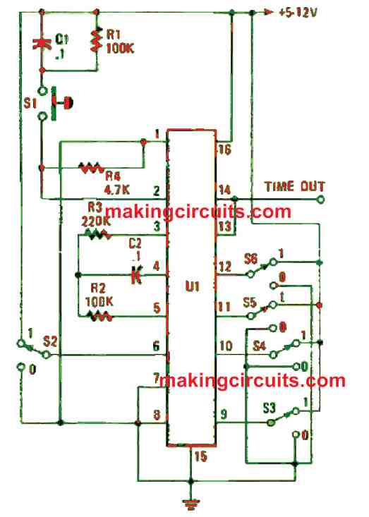
When you press S1, a positive pulse is delivered to the reset, or timer-start input which situates in pin 2 to start the timing cycle. Switch S2 selects the “8-bypass” option while switches S3-S6 configure the binary code for the counters.
When we look deeply into the IC as the schematic from Figure 4, we can see pin 1 is tied high, the decode (out) pin (pin 13) is forced high and the internal oscillator is restricted.
As a result, the circuit is placed in the standby mode. Pin 1 must be attached low for the circuit to be put into the timing mode.
The reset input (pin 2) needs a positive pulse to enable the timer circuit by driving the decode (out) terminal (pin 13) to go low, resetting all the 24 flip-flop stages.
At the point the pulse is positive, the chip’s internal oscillator is inactive. The timing cycle is in an uncertain state until the negative-going edge of the input pulse triggers the timing function.
The in “1” terminal at pin 3 functions as the clock input. The internal counters reach on the negative-going edge of the clock input pulse. An internal oscillator or an external source may drive the clock input.
In the event an external clock is used, both out “1” and out “2” (pins 4 and 5, respectively) may be left detached or used to trigger other CMOS loads.
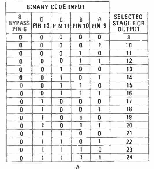
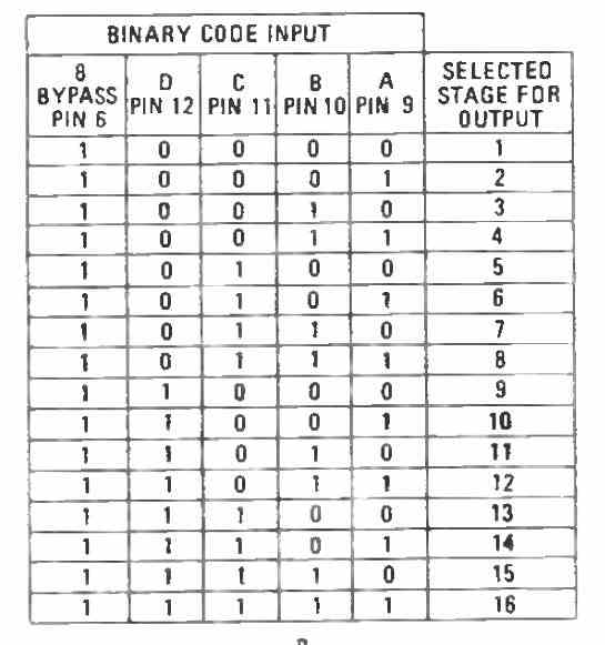
When the 8-bypass terminal (pin 6) is fixed on high, the first 8 flip-flop stages are skipped, enabling the device to be a 16-stage counter with each stage selectable from the 4-bit binary inputs.
As the 8-bypass pin is connected to ground, all 24 flip-flop stages are utilised, with only the final 16 stages chosen by the 4-bit binary inputs. You can check the truth tables in Figure 5 to select and set the binary codes.


The clock-inhibit terminal (pin 7) must be connected to low for standard timing operations. If pin 7 is connected high, the first counter stage will be disconnected from the clocking source. If the input is connected high during a timing interval, the current count will be retained until the input goes negative.
When pin 14 is connected high, the internal RC oscillator halts, decreasing power consumption during standby period. Pin 14 must be connected low for standard timing operations.
The binary inputs (A, B, C and D at pins 9-12) select the number of the counter stages required to configure the needed time delay as shown in the truth tables in Figures below.
The mono-in terminal (pin 15) regulates the operation of the internal monostable multivibrator. This operation of the multivibrator can be ceased when you connect pin 15 to ground.
The multivibrator is triggered by connection a resistor between pin 15 and the +V bus. The resistor;s value and the internal circuit capacitance configure the multivibrator’s timing interval.
This period can also be lengthened by including a capacitor between pin 15 and ground. The resistor values should be in between 5k and 100k. For the capacitor, it must not be more than 1000 pF.
The out “1” and out “2” terminals at pins 4 and 5 are utilised with the in “1” terminal to make an RC-oscillator circuit.
The decode (out) terminal at pin 3 functions as the timer’s output. The circuit shown in Figure 3 displays the frequency of U1’s internal RC oscillator which is set by the same formula deployed in the first timer circuit. You need to set S2 and S3 to the 1 position, and S4, S5 and S5 to position 0.
The bottom Figure 5 displays the binary code for a divide-by-4 function we have selected. You must note that S2 is configured to bypass the first 8-counter stages.
After 4 clock pulses have lapsed, the timer provides a positive input at pin 13. To enable a longer interval, you must set S2 to the 0 position and S3, S4, S5 and S6 to position 1. The oscillator will have to cycle through all 24 flip-flops stages for a count of 16,777,216 before the timer circuit will generate an output.
If the clock is operating at 1 Hz, the timing cycle would count 16,777,216 seconds or 194 days to produce an output.
All you need to do decrease the time delay by a factor of 10 is to increase the oscillator’s frequency to 10 Hz, or a factor of 100 to 100 Hz. The decode (out) terminal at pin 13 is attached back to the oscillator inhibit terminal at pin 14. This disables the oscillator during standby to save power.
If you remove the jumper it causes the timing cycle to repeat continuously as long as power is supplied to the circuit. When you need to apply the timer in the multivibrator mode, you must disconnect pin 15 from low and attach a timing resistor between than pin and the positive supply rail. After that, you must connect a timing capacitor between pin 15 and ground.
Figure 6 shows a bounce-free circuit and it can be connected to the universal programmable timer circuit with pin 4 of the 4011 going to the in “1” pin of the timer. You then need to press S1 to clear and reset the timer circuit.


Every time S1 is pressed, the counter counts up one time. After the total count is reached, the timer delivers a positive output at pin 13.
If a lower frequency is required to power the timer, you may opt for a standard square-wave oscillator circuit as shown in Figure 7.

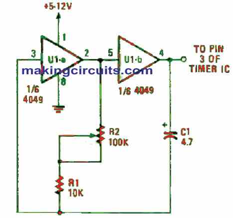
Resistor R2 regulates the oscillator’s frequency and the output pin (pin 4 of the 4049) attached to pin 3 of the timer.