

In the field of power electronics, we sometimes confront an uncomfortable and humiliating fact about ourselves. For a while, I'd like you to attempt to be absolutely open and honest.
Is it possible that you're misinformed regarding the MOSFET body diode?
There are a lot of us. We all have similar genesis tales on how this misunderstanding originated.
MOSFETs have a very important attribute, that is, they would still conduct in reverse despite VGS=0. They achieve this since they have a parasitic diode called an intrinsic body diode between the source and drain. We all learned in power electronics that MOSFETs can conduct in reverse (because to the presence of a body diode) but IGBTs cannot (due to the lack of one).
We just become habituated to calling this phenomenon a "body diode" since "reverse current path with gate off" sounds a lengthy phrase.
And for ages, everything was good.
Then there were new wide-bandgap devices. Many don't have parasitic diodes due to their design. They do, however, possess the same helpful characteristic as MOSFETs: that is when VGS=0, they can conduct in reverse. This characteristic is most notable in GaN E-HEMTs.
A two-dimensional electron gas (2DEG) channel constructed on an AlGaN/GaN hetero-epitaxy structure gives extraordinarily high charge density and mobility in GaN E-HEMTs.
The gate inherently depletes the 2DEG underneath the gate electrode at 0 V, or negative bias, for enhancement-mode functioning. The 2DEG channel is turned on by a positive gate bias that attracts electrons into the depletion region.
This function is due to the MOSFET's forward conduction (first quadrant), but with superior switching efficiency.
The device starts working differently when a MOSFET is in the third quadrant (VGS =0, VDS negative). In simple sense, a voltage gradient in the device channel is created by a negative bias on the drain pin of the device.
This results in a negative electrical potential in the depletion zone under the gate with respect to the gate electrode. To put it another way, the GaN HEMT drain will work as the source, and the source will work as the drain.
The transistor is switched on when the potential difference across the gate and the channel surpasses the threshold voltage (VTH GD) of the transistor, a phenomenon known as "self-commutation."
The voltage drop D is caused by the device conducting current, I, via its (resistive) channel, Ron.
It is expressed as:
D = VTH_GD + IRon
As soon as the MOSFET is switched off with a negative voltage, the drain becomes even more negative before self-commutation occurs, resulting in a total voltage drop DT, which can be expressed as:
DT = VTH_GD + (-VGS) + IRon
So What's the Confusion
Are you confused regarding what is the actual use of the internal body diode in all modern MOSFETs? Well, actually to be precise they have no use at all, since all the modern FETs today are designed in such a way that current is able to flow across source to drain whenever these are reverse biased.
The intrinsic body diodes are symbolically illustrated in the figure below as a cross-section of an N-channel enhancement-mode MOSFET. The diodes in these MOSFETs point from the body to the drain and source. Because it is short circuited by an internal body to source contact, the body to source diode is typically meaningless.

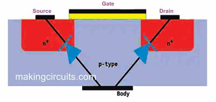
Such diodes are aptly called body diodes, since these are inherent to all FET types but apart from JFETs. Between the substrate and the doped portions of the FET structure, we have the P-N junctions located.
Due to the obvious polarity of the body diode, current flows from the drain to the source in N-channel FET implementations. Current could still pass across the source to the drain through the shorted source to body link and the body to drain diode even if a channel has still not been biased. As a result, a normal N-channel FET is unable to prevent current passage from the source to the drain.
The body diode is indeed dependent on with regular circuit functioning in some designs, for example in many DC-to-DC converters. In some applications, like certain power source selectors, wherein current should be interrupted in both channels, this increases the number of FETs required.
The internal BJT (Bipolar Junction Transistor) within the FET is likewise created by a couple of back-to-back P-N junctions; although, with a shorted body to source connection, this effectively eliminates.
Some more Facts Regarding MOSFET Body Diodes
The mosfet body diode is there to safeguard half-bridge applications by allowing the low-side BEMF inductive turnoff (+ spike) to pass through the high-side diode to Vdd.
The diode structure appears to have been introduced on purpose. Because we employ junction isolation to isolate the source and drain from the body and from each other, the diode is really included into the design of most MOSFETs.
To avoid the body voltage from affecting the threshold voltage on 3-terminal MOSFETs, the body must be connected to the source. A body diode is not present in MOSFETs made with silicon on insulator (SOI) technology.
The p-n junction between the MOSFET's body and the drain is known as the intrinsic body diode. For simplicity, the source and body of a solitary (standalone) MOSFET are frequently linked together to form a 3-pin package. This indicates that a diode exists between the source and the drain of the device.
The diode continues to be switched off when the source voltage is always lower than the drain voltage, and all functions as intended. This implies you CANNOT (simply) switch a bidirectional signal using a MOSFET. This constraint isn't a huge concern in reality because discrete MOSFETs are virtually usually utilized for low-side switching.