This post is a research layout report for the 1.44 W non-isolated buck converter by using LinkSwitch™-TN2 LNK3204D/P/G, which can be effectively implemented as a 220V to 12V 100mA SMPS transformerless power supply circuit.
It typically works at an input voltage which range from 85 VAC to 265 VAC and offers an output of 12 V at 120 mA.
This particular research design attributes extremely integrated alternative, most reasonable component count, no optocoupler or Zener diode necessary for regulation, heat overload security along with automativ restoration, <30 mW no-load utilization, > 75% efficiency at total load, and ±3% load regulation. It is absolutely ideal for LED driver applications.
The data provides the power supply specs, schematic, parts list, PCB layout, and functionality info.
Circuit Description
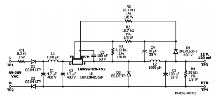
The schematic exhibits a buck converter employing LNK3204D/P/G. The circuit offers a non-isolated 12 V, 120 mA constant output.
LinkSwitch-TN2 combines a 725 V MOSFET and control circuitry perfectly into a single affordable IC. Stabilization is accomplished by using a inexpensive resistor divider network feedback.
The switching frequency burst characteristic of the LinkSwitch-TN2 family and the 66 kHz switching frequency of functioning allows minimizing EMI.
Input EMI Filtering
The input stage is made up of fusible resistor RF1, diode D1 and D2, capacitors C1 and C2, and inductor L1. Resistor RF1 can be a flameproof, plomos, wire-wound resistor. This achieves a number of capabilities: (a) restricts surge current to harmless degrees for rectifiers D1, D2 (b) supplies differential mode noise cancellation and © acts as an input fuse in case any additional component does not work out and short circuit.
To face up to the immediate inrush power challenge, wire wound varieties are encouraged. Metal film resistors are generally not advised instead of RF1.
LinkSwitch-TN2 combines a 725 V power MOSFET and control circuitry into a solitary cheap IC. The unit is self-starting through the DRAIN (D) pin using localized supply decoupling offered by a tiny 100 nF capacitor C3 coupled to the BYPASS (BP/M) pin while AC is initially put on.
In the course of usual operation, the unit is driven from output by using a current limiting resistor R3. In this article, the unit LNK3204D is employed in a buck converter.
The proposed 12V 100mA SMPS transformerless power supply circuit is developed to perform in typically discontinuous conduction mode (MDCM), using the peak L1 inductor current fixed by the LNK3204D inner current limit.
The control plan employed is comparable to the ON/OFF control found in TinySwitch™. The on-time for every switching cycle is defined by the inductance value of L2, LinkSwitch-TN2 current limit as well as the high voltage DC input bus over C2.
Output regulation is achieved by bypassing switching cycles in effect to an ON/OFF feedback transmission placed on the FEEDBACK (FB) pin. This may differ considerably from standard PWM strategies which regulate the duty factor (duty cycle) of each switching cycle.
As opposed to TinySwitch, the logic of the FB pin may be upside down in LinkSwitch-TN. This enables an easy feedback system to be applied as soon as the device is utilized in the buck converter setup.
Current on the FB pin higher than 49 µA may prevent the switching of the interior MOSFET, although current lower than this permits switching cycles to take place.
Courtesy: https://ac-dc.power.com/design-support/reference-designs/design-examples/rdr-506-144-w-non-isolated-buck-converter/?AdSource=EEWeb