


A circuit that uses a programmable Arduino-based oscillator to generate a three-phase AC output is known as an Arduino three-phase inverter.
In order to operate a specific three-phase load, we may learn how to build a basic Arduino-based microcontroller three-phase inverter circuit in the following section. This circuit can be enhanced depending on individual preferences.
Introduction to the 3 Phase Inverter Circuit
In one of our earlier posts we delved into an effective yet simple three phase inverter circuit that made use of operational amplifiers to generate the three phase square wave signals.
At the same time the three phase push pull signals that were necessary for driving the MOSFETs were implemented using specialized three phase driver integrated circuits.
Current Concept Overview
In the current concept we are also configuring the main power stage by utilizing these specialized driver integrated circuits.
However this time around we are creating the three phase signal generator with the help of an Arduino.
Complexity of Arduino Based Drivers
Now you might be wondering why we chose to go this route.
The reason is that designing an Arduino based three phase driver can be extremely complex and it is generally not recommended for most applications.
Additionally it is significantly easier to obtain off-the-shelf efficient digital integrated circuits for this purpose at much lower costs.
Next Steps
Before we dive into building the complete inverter circuit it is essential that we first program the following Arduino code into an Arduino UNO board.
Once that is done we can proceed with all of the remaining details.
Arduino 3 Phase Signal Generator Code
#define PHASE_A 13
#define PHASE_B 12
#define PHASE_C 8

const int delayTime = 3333; // Microseconds for precise phase shifts (3.33ms)

void setup() {
  pinMode(PHASE_A, OUTPUT);
  pinMode(PHASE_B, OUTPUT);
  pinMode(PHASE_C, OUTPUT);
}

void loop() {
  digitalWrite(PHASE_A, HIGH);
  digitalWrite(PHASE_B, LOW);
  digitalWrite(PHASE_C, LOW);
  delayMicroseconds(6670); // Initial 6.67ms delay

  digitalWrite(PHASE_B, HIGH);
  delayMicroseconds(delayTime);

  digitalWrite(PHASE_A, LOW);
  delayMicroseconds(delayTime);

  digitalWrite(PHASE_C, HIGH);
  delayMicroseconds(delayTime);

  digitalWrite(PHASE_B, LOW);
  delayMicroseconds(delayTime);

  digitalWrite(PHASE_A, HIGH);
  delayMicroseconds(delayTime);

  digitalWrite(PHASE_C, LOW);
  delayMicroseconds(delayTime);
}
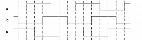
The following figure may be used to display the hypothetical waveform applying the code mentioned above:

It's time to proceed and setup the various additional circuit stages after you have burnt and verified the aforementioned code in your Arduino.
You shall require the following components for this, something that you may currently have:
Parts Needed
| Component | Quantity | Notes |
|---|---|---|
| IC IR2112 (or similar 3 phase driver IC) | 3 nos | |
| BC547 Transistors | 3 nos | |
| Capacitor 10uF/25V | 3 nos | |
| Capacitor 1uF/25V | 3 nos | |
| Capacitor 100uF/25V | 1 no | |
| Diode 1N4148 | 3 nos | Recommended over 1N4007 |
| Resistors | All 1/4 watt, 5% tolerance | |
| - Resistor 100 ohms | 6 nos | |
| - Resistor 1K | 6 nos |
Building Specifics
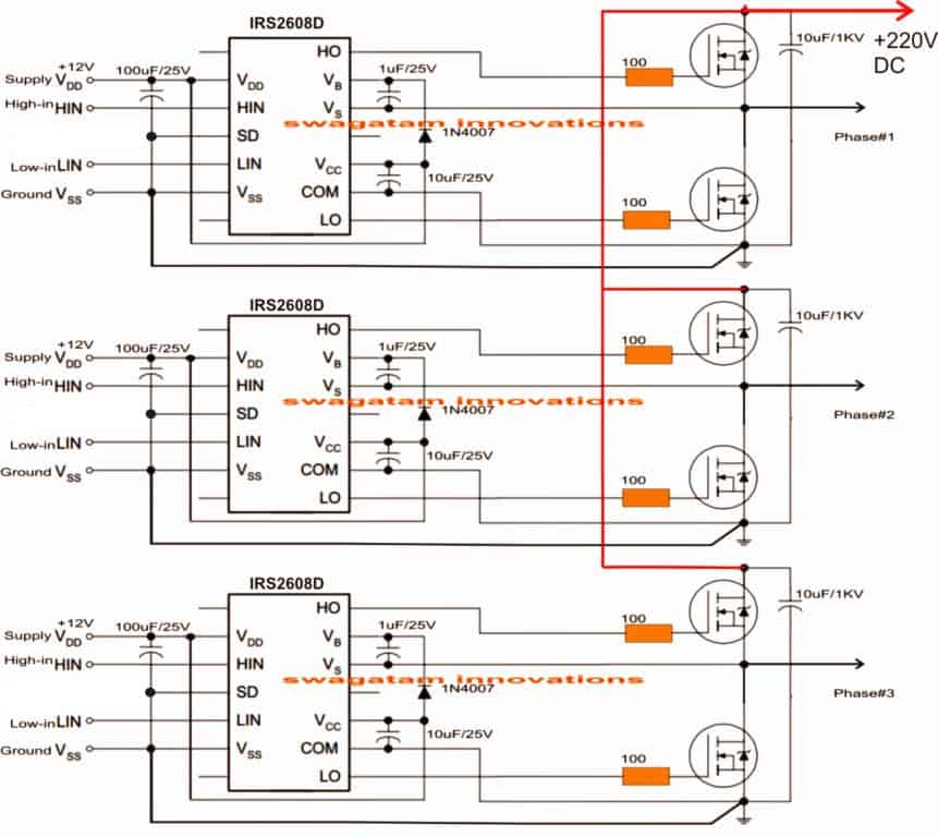
First, as shown below, we connect the three ICs to create the desired three-phase mosfet driver stage:

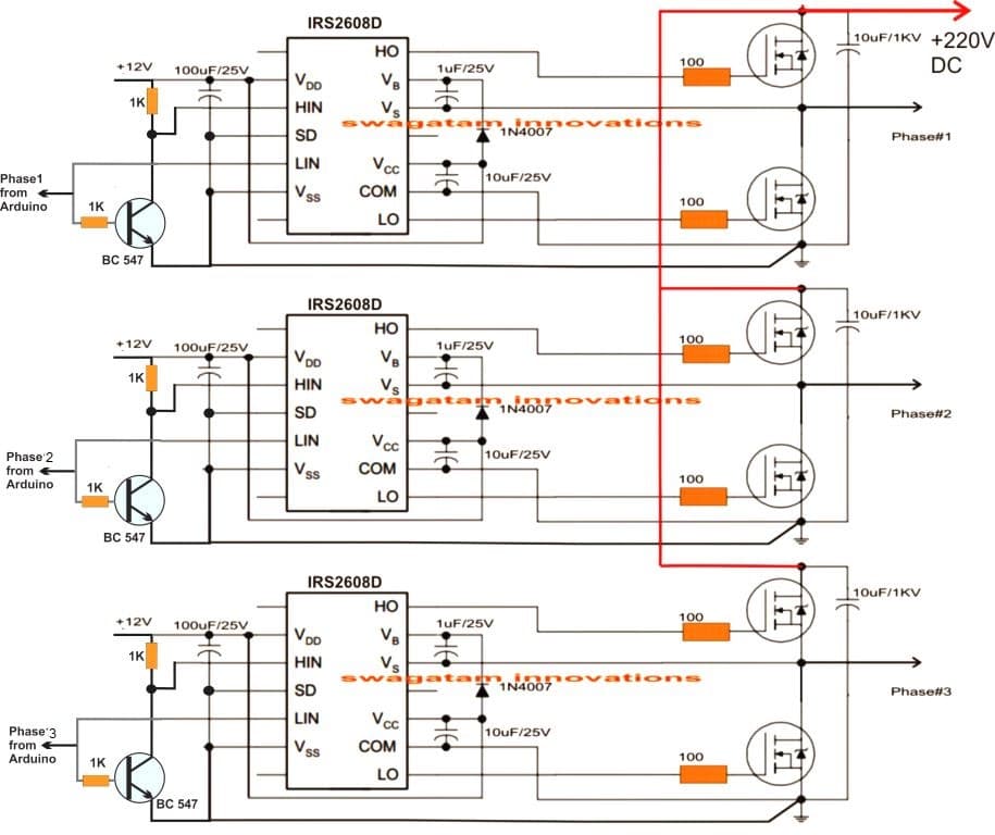
The BC547 transistors are connected to the IC's HIN and LIN inputs soon after the driver board is put together, as shown in the accompanying figure:

Verifying the Designs
After you have constructed the designs mentioned above you will be able to quickly verify the intended result by simply switching on the system.
It is important to remember that the Arduino requires a little bit of time to boot up.
Therefore it is highly recommended that you switch on the Arduino first and then after waiting for a few seconds proceed to switch on the +12V supply to the driver circuit.
Calculating Bootstrap Capacitors
As we observe in the figures provided earlier the circuit necessitates a couple of external components situated near the MOSFETs.
These components take the form of diodes and capacitors.
They play an essential role in facilitating precise switching of the high-side MOSFETs and this entire setup is referred to as the bootstrapping network.
Although the values of these capacitors have already been indicated in the diagram they can be specifically calculated using the following formula.
C >= 2 * [(2 * Qg) + (Iqbs(max) / f) + Qls + (Icbs(leak) / f)] / (Vcc - Vf - Vls - Vmin)
Where:
Qg = Gate charge of high-side FET
f = Frequency of operation
Icbs(leak) = Bootstrap capacitor leakage current
Iqbs(max) = Maximum Vbs quiescent current
Vcc = Logic section voltage source
Vf = Forward voltage drop across the bootstrap diode
Vls = Voltage drop across the low-side FET or load
Vmin = Minimum voltage between Vb and Vs
Qls = Level shift charge required per cycle (typically 5 nC for 500 V/600 V MGDs and 20 nC for 1200 V MGDs)
How to Calculate the Bootstrap Diodes
When it comes to figuring out how to calculate the bootstrap diodes there are a few important things to keep in mind.
The equations mentioned earlier can definitely help you determine the right capacitor value for the bootstrap network.
However when it comes to the diode associated with this setup there are some specific criteria that we need to consider.
Understanding Diode Activation
The diodes in this scenario become active or enabled when they are in forward bias mode.
This happens when the high side MOSFETs are turned on and at that point the potential around these components is nearly equal to the BUS voltage that spans across the full bridge MOSFET voltage lines.
Because of this it is essential that the bootstrap diode is rated appropriately so that it can effectively block the full applied voltage as specified in the diagrams that you might be working with.
Current Rating Calculation
Now while this may seem straightforward calculating the current rating for the diode does require a bit of math.
You will need to multiply the gate charge magnitude by the switching frequency to arrive at the correct value.
For instance if you happen to be using the MOSFET IRF450 with a switching frequency of 100 kHz you would find that the current rating for the diode would be approximately 12 mA.
This number appears quite low and most diodes typically have much higher current ratings than this so you may not need to worry too much about it.
Over Temperature Leakage Consideration
However it is important to note that the over temperature leakage characteristics of the diode should not be overlooked.
This becomes particularly crucial in situations where the bootstrap capacitor is expected to hold its charge for a reasonably extended period of time.
In such cases it is advisable to use an ultra-fast recovery type diode.
This helps minimize any unwanted charge from being pushed back from the bootstrap capacitor towards the supply rails of your integrated circuit.
Some Safety Tips
As we all know MOSFETs used in three-phase inverter circuits can be quite susceptible to damage due to various risky parameters that come into play with these concepts.
This is especially true when dealing with inductive loads.
I have previously discussed this topic in detail in one of my earlier articles and I highly recommend that you refer to that article for guidance on how to implement MOSFETs according to best practices.
Using IC IRS2330
Now let us talk about using IC IRS2330.
The diagrams provided are designed specifically for creating a three-phase PWM controlled inverter using an Arduino as your controller.
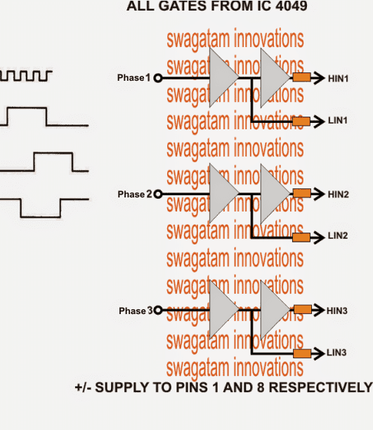
In the first diagram you will see that it is wired using six NOT gates from IC 4049.
This particular stage serves the purpose of bifurcating the Arduino PWM pulses into complementary high and low logic pairs.
This setup ensures compatibility with the bridge three-phase inverter driver IC IRS2330 when fed with those PWM signals.


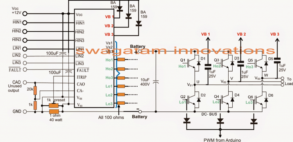
The second diagram we discussed earlier is all about the bridge driver stage for our exciting Arduino-based PWM three-phase inverter design and it prominently features the IRS2330 bridge driver chip.
Now let us break it down a bit!
The inputs on this nifty little IC are labeled HIN and LIN.
These inputs are designed to receive the PWM signals from our Arduino which have been processed through NOT gates.
Once these signals are in the IC gets to work driving an output bridge network made up of six IGBTs.
These IGBTs then power the connected load across their three outputs making everything come to life!
Moving on to some finer details we have a 1K preset resistor in play here.
This little component is crucial for setting the overcurrent limit of our inverter.
By adjusting it appropriately across the shutdown pin of the IC we can ensure everything runs smoothly.
If you find yourself needing a bit more juice and are looking at higher current specifications for your inverter you might also consider reducing the 1-ohm sensing resistor a tad.
Wrapping Up:
And there you have it!
This wraps up our deep tutorial into building an Arduino-based three-phase inverter circuit.
If you have any lingering questions or need clarification on anything we covered do not hesitate to drop a comment below.
We are here to help and will get back to you in no time!
For the PCB Gerber Files and other related files you can refer to the following link:
https://drive.google.com/file/d/1oAVsjNTPz6bOFaPOwu3OZPBIfDx1S3e6/view?usp=sharing
The above details were contributed by "cybrax"