

We know that a design using complimentary emitter follower transistor significantly increases the output power of an operational amplifier.
Similarly for achieving highly increased output power MOSFETs amplifier can be designed as complimentary source follower.
However, this would also result in the maximum output voltage getting reduced significantly by the gate source of the MOSFET by a couple of volts.
How the Circuit Works
Connecting two MOSFETs as a complementary drain follower could also be used. The level of the supply voltages and the saturation voltages of T3 and T4 limits the output current provided by the MOSFETs.
Resistor R8 and R9 are responsible for providing feedback for the opamp and the MOSFETs. There is an increase in the open-loop amplification of the opamp by (1+ R8/R9). (1+R3/R2) is the closed-loop amplification of the complete amplifier.

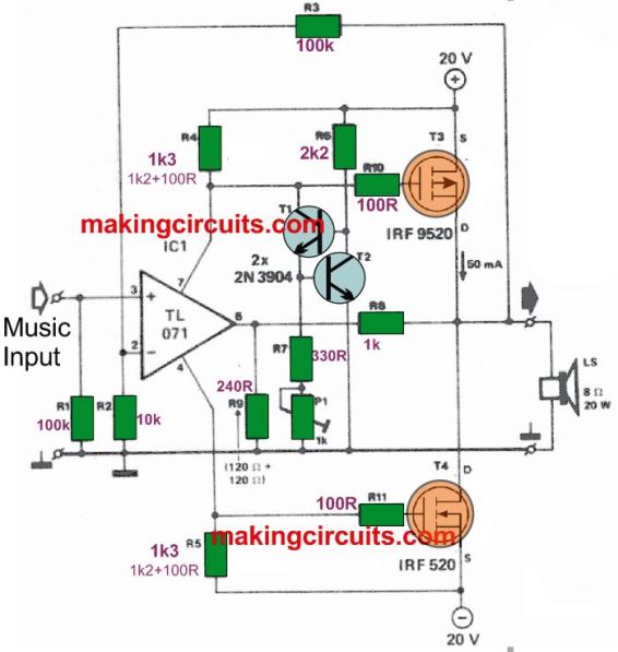
The arrangement of quiescent current of T3 and T4 at 50mA is completed but the current source formed by T1 and T2.
The direct current through the opamp resulting in the voltage drop across the resistors should not be sufficient to switch onT3 and T4, so the values of R4 and R5 should be regulated.
The rise in the voltages across R4 and R5 increases the quiescent current through T3 and T4, depending on the setting of P1 and depending on the current source.
T2 must be mounted on the common heat sink (c. 5 K/W) of the MOSFETs, in view of the temperature dependence of the quiescent current.
In this simple MOSFET amplifier design the harmonic distortion is equal to 0.075 percent at 100Hz and to 0.135 per cent at 10kHz when the output power is not less than 20W into 8 Ohm.