


The digital sinewave oscillator is a device used for generating sinusoidal sinewave signals using digital logical signals.
The oscillator circuit has two sections, which also have their own useful applications. Design of the two sections are, an oscillator around a pair of exclusive OR gates and a circuit divided in three parts that is in between of two ordinary flipflops.


An inverting(N1) and a non-inverting(N2) gate is used to design an oscillator. A non-inverting gate is made up of two inverting gates in series connection. So, using only inverting gate three would have been required to complete the circuit.
Working of Circuit
It is assumed that input of N1 (pin2) is low initially. Thus, output of N1 is also low but the output of N2 is high. Resistor R2 charges the capacitor C1. After sometime, input of N1 goes from low to high via the R1 resistor and the whole process reverses.
Readers wanting to dive deep in these types of oscillators can refer to the National Semiconductor Application Note No. AN-118, which can be found in their current CMOS data book.
The section of circuit divided into 3 parts that consisted of two flip flops is divided by two. All together they would be divided by four. In between the output of FF2 and input of FF1 another EXOR gate named N3 is included. Each time the output of FF2 changes, the polarity clock input signal is inverted.
The output of flipflop would not have changed till the end of current clock period in the absence of N3. The flipflop is triggered by a positive-going edge after every half period and the clock signal becomes negative after N3 is added. The dividing factor now changes from four to three.
A pair of resistors named R3 and R4 generates the sine wave signal. The output voltage depends on both the inputs. It will be high(= logic 1) if both of the inputs are high and low(= logic 0) if both of the inputs are low. But, it will be ¾ or ¼ of the supply if one of the inputs is high and the other is at low level.
Digital Sine Waveform Image
The above logic can also be proven mathematically but for better understanding a single sine wave period is examined diagrammatically.

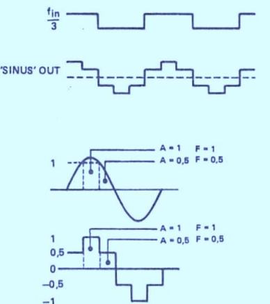
For this purpose three small rectangles of the same size are drawn in the sine wave. Rectangle represents a logic one level. One rectangle is drawn in the center and the other two vertically at each side of the rectangle.
It can be observed that the area covered by sine wave to the rectangle is exactly half as compared to the area covered by sine wave to the rectangle at the center. The similar signal figure can be generated when digital simulation technique is used.
It should be taken care while constructing the digital sinewave generator circuit, pins 12 and 13 of the EXOR chip (N4) should be grounded (0V). Alternatively saying, CMOS input should never be floating in the circuit.