Considering adequate decoupled supply rails is extremely crucial in all logic circuits when constructing a digital circuit, failing which could be a costly and hazardous mistake.
The two principal factors that validate the importance of decoupling is the introduction of the fast HC and HCT series of CMOS logic chips, and the readily available dynamic Ram (DRAM) components.
Being fairly low in price, the integrated circuits 41256256 Kbit DRAM and 6264 CMOS SRAM are frequently found in many applications.
The increasingly popular demand for the new CMOS series of logic circuits has produced rumours that these chips are deployable without much attention to the decoupling of the supply lines.
Nevertheless, the devices have significantly low current consuming properties than TTL components. Sadly, it has encouraged electronic enthusiasts to unethically spare or completely disregard decoupling requirements.
Why Decoupling is required in Logic Circuits
The operation of a logic circuit works as the current consumption of the TTL components are dissipated mainly by the resistors. CMOS devices are exclusive, and they do not consume any current in the ‘non-operating’ mode.
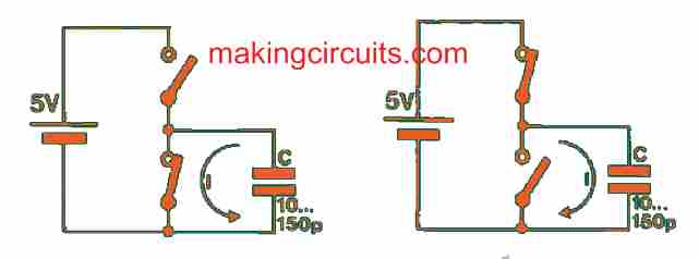
Whenever switching activity by the TTL and CMOS circuits takes place, the capacitance’s charge will have to be reversed as shown in Figure 1.

The internal switching currents of the IC are just a portion of what is needed for the load capacitance and therefore can be disregarded.
Exception, however, is made for circuits that use counters.
An identical peak current is consumed by TTL and CMOS circuits when the switching operation happens.
Why Decoupling Capacitor is Connected Directly with the Supply Rails
The reason why decoupling capacitors are installed directly to the IC supply terminal is that they hold the instantaneous supply voltage from dipping to an undesired level during switching.
The connection between capacitor-to-package distance and the peak amplitude of the spikes on the power supply to a standard HCMOS gate is represented in Figure 2.

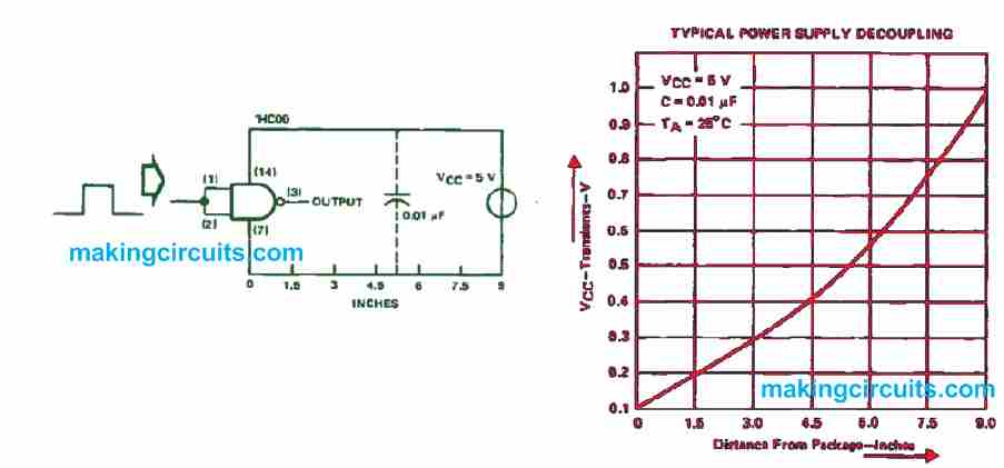
This confirms that the decoupling capacitors must be installed extremely near to the IC supply terminals to alleviate the residual inductance of the supply tracks on the PCB regardless of how good they are imprinted.
There are cases where customized circuits come with long supply tracks and misplaced decoupling capacitor.
As a result, spikes are exposed to ringing effects that impede the general operation of the circuit.
Track Layout to Prevent Oscillations
As a countermeasure, many paths on the PCB were suggested if placing the decoupling capacitor near to the IC is not achievable. This method is called the grid structure and preferred over thick, individual tracks as shown in Figure 3.


Depending on the identifiable number of IC outputs that are concurrently active, the decoupling capacitor’s value must be determined. Usually, you can start with 20 to 100 nF for every three ICs.
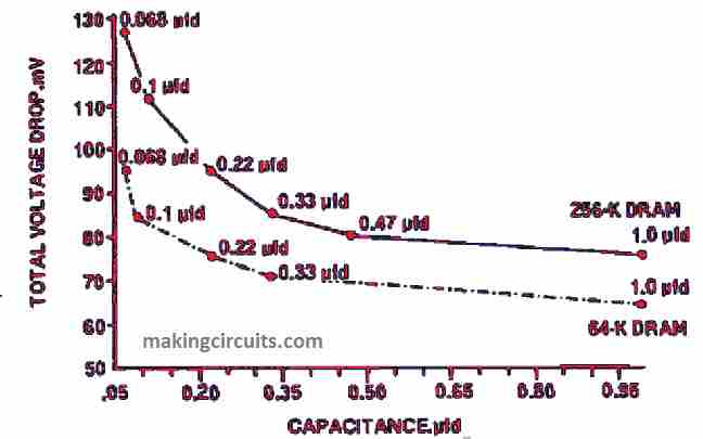
While experimenting, it was noted that decoupling of the 256 Kbit DRAM is more challenging than a 16 Kbit DRAM.
Nevertheless, that isn’t a big problem because manufacturers ensure the size of the chip carrier is compacted thus lessening the freeloading capacitance.
Main Advantage of Decoupling
Their main objective is to make sure the devices accomplish optimal response at high frequencies.
Although some say the value of 330 nF is recommended as depicted in Figure 4, there has been no complaint when with 100 nF decoupling capacitors.