

If you ever be in a mood to build a strong yet simple mobile transceiver and, simultaneously wish to understand surface mount technology (SMT), this is actually the project for a person like you!
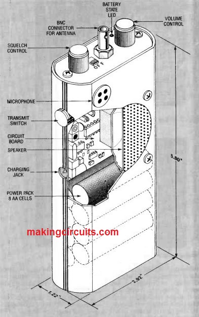
The E-Comm frequency modulated (FM) transceiver is encased within a robust yet eye-catching metal box smaller than 6 inches in length.

Transmitter Diagram

It is among the most unconventional transmitter/receivers ever created for its power quality and working frequency range. The enclosure incorporates a standard rechargeable nickel - cadmium power pack that should help you save the expense of frequently changing eight AA alkaline cells.
The E -Comm receiver features a excellent 0.3 microvolt sensitivity (12 -dB SINAD) for excellent reception, as well as its transmitter provides you with a minimum of a 90% performance. E -Comm owes its efficiency to its revolutionary Class -E final amp that displays substantial power gain.
Receiver Diagram


It gives a consistent output of 3 watts rms into a 50 ohm antenna or dummy load. The economical receiver and the rechargeable power supply have the ability to maintain E -Comm within the air in the squelch mode -for 80 hrs without the need of recharging the power pack.
Designed for narrow -band FM, E Comm features a functional carrier frequency range of 27 MHz to 32 MHz with just crystal and alignment adjustments. The topic of this post is really a edition created for 27.145 -MHz functioning. Using improvements to the transmit and receive filters (part value variations) working approximately 60 MHz is achievable.
This makes it possible for the transceiver to perform both the six- and ten - meter amateur radio wavelengths. Note: This transceiver hasn't been registered for FCC agreement, and its functioning in specific radio frequencies probably are not permitted and/or may necessitate certification.
The top board regulates of E Comm consist of an ON-OFF switch, VOLUME and SQUELCH buttons plus an LED power -pack voltage level indication. The detachable seven-inch antenna is combined into the transceiver using a 50 -ohm bayonet -style BNC connector connector. Each of the components other than the battery pack, microphone, and speaker are attached to the double-sided PC board.
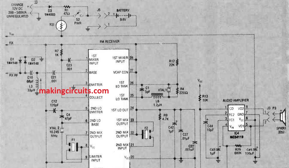
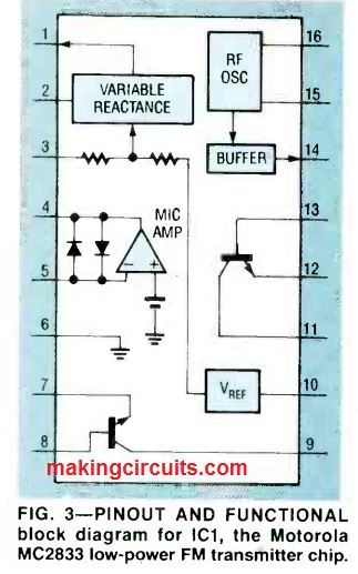
Substantial utilization of ICs and SMD parts makes it possible for the circuitry to adjust to on a PC board that will gauge only 2.25 x 3.1 inches. Just how it had been developed The transceiver features 3 most important stages: transmitter, receiver, and power supply. (Refer Figs. 1 and 2.) The transmitter is created using Motorola's MC2833, which is a low power FM transmitter IC whose pinout and functional block diagram are shown in Fig. 3.

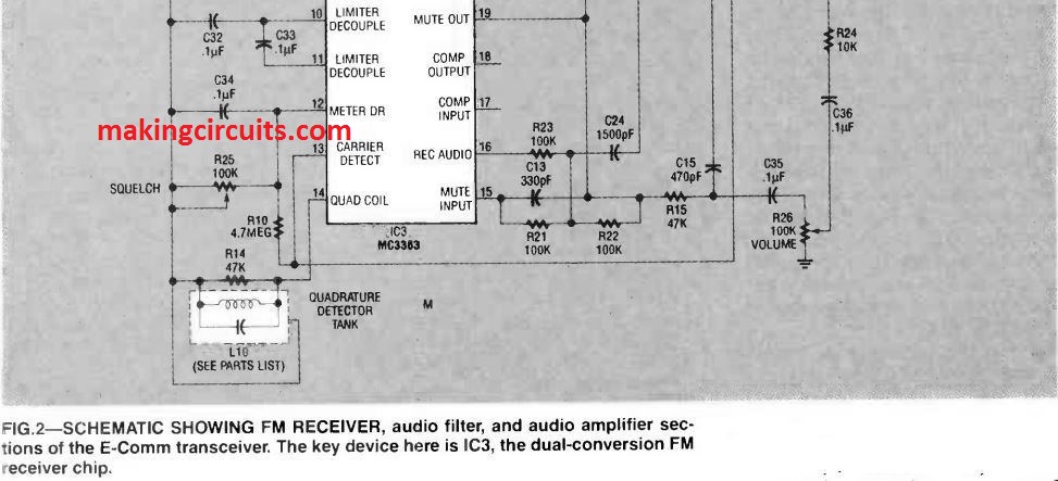
The receiver is developed through the Motorola's MC3363, a low power, double conversion FM receiver IC as their pinout and block diagram can be witnessed in Fig. 4.

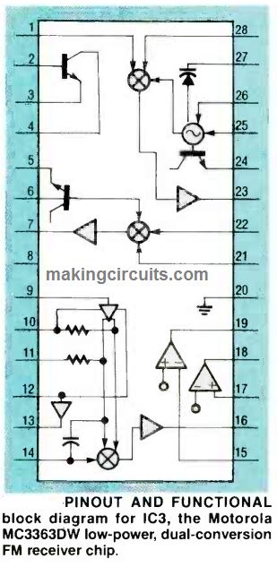
Signals detected by the antenna are preselected through the 5 pole transmit bandpass filter which involves inductors L4, L7, and L5 and capacitors C11, C2, and C30 as indicated on the right side of Fig. 1. The received transmission is now sent via the receive/transmit switch S1 -b to an impedance matching stage comprising C10 and L3 displayed on the left of Fig. 2.
This stage delivers an extra 2 poles of preselection. Diodes D1 and D2 protect against overloading and the likely damage of the RF amplifier transistor in case it is encountered with overdriving at the front end. The preselected transmission is subsequently amplified by the IC3 (MC3363) internal common-emitter RF amplifier stage and given to the 1st mixer stage on pin 1. The RF amplifier comes with a gain of around 20 dB.
The 1st local oscillator (LO) pulls a 3rd overtone from a crystal, and runs the 1st mixer by using a inner cascode amplifier.
Down conversion helps make the 1st LO frequency (the first IF frequency) 10.7 MHz higher than the carrier. For instance, if a 27.145 MHz carrier had been existing, the crystal frequency could be 27.145 MHz in addition to 10.7 MHz or 37.845 MHz. The mixer is actually a two times as balanced multiplier that delivers around 18 dB of conversion gain. The output of the mixer is an emitter-follower stage having an output impedance of 330 ohms to complement the ceramic filter.
Filter F2, a 10.7 MHz ceramic bandpass filter, gets rid of undesirable out-of-band harmonics from the output of the 1st mixer. The 2nd mixer pulls out a signal from the 10.245 MHz fundamental mode crystal controlled oscillator XTAL2 whose output is combined with the 10.7 MHz first IF to create the 455 kHz 2nd IF having a conversion gain of roughly 21 dB.
The 455 KHz ceramic filter F1 (on the left of IC3) supplies narrow band filtering for the limiter amplifiers within IC1, the MC2833 FM transmitter IC. The limiter stage snip the 455 kHz second IF signal to eliminate undesirable amplitude modulated signals and link with the audio detector.
A quadrature detector inside IC3, the MC3363, picks up the modulated signal. The parallel quadrature detector tank, L10, inside the detector is fine alligned to 455 KHz. The demodulated (audio) transmission at pin 16 of the FM transmitter ICI is subsequently cleaned by an active filter stage that consists of an op amp inside of IC3, the FM receiver chip in Fig.2.
This active filter, hooked up at pins 15 and 19 of IC3 and composed of capacitors C13, C24, and C15 and resistors R21, R22, R23, and R15, features a cut off at 3 kHz Squelch is carried out through the carrier sensing functionality on pin 13 of the FM transmitter IC, IC1 in Fig. 1.
Resistor R10 (in between pins 12 and 13) delivers hysteresis within the squelch circuit in order to avoid unnecessary "shoot through." This squelch circuit is unconventional; its output together facilitates and disables IC4, a Motorola MC34119D low power audio amplifier which has a CHIP DISABLE pin 1 (CD).
Power usage is minimized by turning off the audio amplifier should the receiver is squelched, plus its additionally held low since it is operated through the un-controlled power supply along with the 32 ohm speaker.
This particular set up retains receiver consumption just at 7 mA from the battery pack once the receiver is in the squelch mode. The gain of the audio amplifier is defined by resistor R29 (in between pins 4 and 5) and neighboring resistor R24, and is also indicated as (2 x R29/R24).
How Transmitter Works
The transmitter is actually a 3 watt narrow band FM Class E circuit having an efficiency output better than 90%. IC1 forms the heart of the front end of the transmitter, the low power FM transmitter IC.
The speech transmission is detected by the microphone and supplied to the MIC AMP INPUT on pin 5 of IC1. Resistor R11 (in between pins 4 and 5) fixes the amplifier gain, and the output of the amplifier operates the FM modulator.
An adjustable reactance within the modulator "twists" the crystal frequency controlled oscillator stage. Since deviating the crystal frequency isn't possible by around some kilohertz through the adjustable reactance circuit, a multiplication design extracts the appropriate carrier and modulation frequencies. In the E -Comm. a crystal frequency corresponding to 1/3 carrier frequency had been decided on.
Inductor L9 (in series with XTAL3 in between pins 1 and 16 of IC1) fine tunes the oscillator frequency in the absence of a modulation supply. The oscillator buffered output on RF OUTPUT pin 14 subsequently supplies a tank circuit consisting of inductor Ll and capacitor C8, that is aligned to the 3rd harmonic of the oscillator.
The transmission is increased with a factor of 3 to get the carrier frequency within this tank circuit. The carrier and the modulation signal together are multiplied to acquire the 5 kHz deviation demanded by the receiver.
After this, the signal is transferred via a tuned common emitter amp to boost and soften the carrier. The MOSFET output turns with the antenna impedance along with the filtering process.
Variable capacitor C30 adjusts the output stage to match up the antenna or dummy load. Observe that for getting class E working, both the load and the multiplier stages has to be adjusted relative to guidelines within the Calibration and "lineup section of this article.
Mismatch and overload security are offered through Zener clamp D4 (Fig.1, between Q1 and 92) along with the Poly button protective resistor R31 (Fig. 2, top left) in the power supply.
The low voltage regulator demonstrated in Fig. 1 features a CMOS voltage regulator IC5, a Maxim MAX666, that sustains power and supplies a couple of capabilities: reduced quiescent current of approximately 15 uA and a pre-installed low battery sensing feature.
The regulated output is determined by resistor R18 (pin 6) and R28 at 6.4 volts.
This magnitude of voltage had been decided to deliver sufficient gate voltage to turn ON MOSFET's 91 and 92 optimally without the need of exceeding the absolute maximum voltage specs of the quad NAND gate IC2. The low battery sensor circuit is determined by resistors R17 and R30 at LBI pin 3 of IC5 to approximately 8 volts.
Due to the fact the voltage regulator is a CMOS device, resistor with higher values are positioned in the feedback loops for additional decrease of power usage. Pin 7 of IC5 LBO comes with an open drain output that runs the low battery warning LED1.
The receive/transmit switch S1a transforms the receive and transmit stages of the transceiver on / off for added power efficiency. The power pack includes 8 AA nickel cadmium rechargeable cells, each rated at 1.2 volts at 500 mA hours. The pack is recharged via connector J2 (Fig. 1, top left) by a 120 volt AC to 12 V DC adapter connected to the AC line.
Constructing the transceiver using SMD


Surface mount devices (SMD) have been preferred for E -Comm simply because they encourage the structure of a smaller transceiver, and their tiny part dimensions make sure that PC board footprints are short.
As a result, constructing this transceiver you'll receive a heads high on the entire technique of surface-mount technology (SMT) since you may obtain hands-on expertise in choosing and inserting the mini parts and an consciousness of both the advantages and downside of SMT.
Having said that, never try to build this transceiver if you are not yet an established project builder.
Numerous SMD elements aren't designated with numbers or scores mainly because of the constrained space on their housing. Because of this it is necessary to be particularly cautious to prevent confusing chip elements prior to and through the construction. Professional equipment must be employed in picking and inserting SMD parts.
They must be well suited for gripping tiny, difficult to handle components. Recommended ones are stainless tweeezers having needle point curved-end for picking and placing small parts for example chip resistors, capacitors and diodes within the PCB. Sharp pliers as used by the jwellers will probably be helpful for styling stub leads on surface-mount IC's.
Carry out all soldering using a high-quality pointed 10- to 15 -watt pencil type soldering iron. A lit up magnification glass will probably be beneficial, ideally one which brackets around the border of a table.
Don't use anything but premium quality fine (0.01- to 0.02 -inch) diameter solder wire along with an appropriate liquid flux. Maintain fine solder eliminating desolder wik readily available to mend any kind of errors you could possibly make.
Anybody developing E -Comm must be psychologically ready for the remarkably tiny scale of the SMD parts and their close spacing. Dealing with SMD parts requires next to professional grade soldering abilities and plenty of endurance.


Parts List
Resistors (All 1206 SMD chip resistors are 1/8 -watt, 5%, unless
otherwise specified)
R1-47 ohms, 1/2 -watt, 5%, radial - lead
R2-22 ohms, 1206, SMD
R3-47 ohms, 1206, SMD
R4-220 ohms, 1206, SMD
R5-330 ohms, 1206, SMD
R6-470 ohms, 1206, SMD
R7-1000 ohms, 1206, SMD
R8, R9-4700 ohms, 1206, SMD
R10-4.7 megohms, 1206, SMD
R11, R12-22,000 ohms, 1206
SMD
R13, R24-10,000 ohms, 1206
SMD
R14, R15-47,000 ohms, 1206
SMD
R16 -R23-100,000 ohms, 1206
SMD
R25, R26-100,00 ohms potentiometer, Bourns 51CADD12A20,
or equivalent
R27-330,000 ohms, 1206 SMD
R28-390,000 ohms, 1206 SMD
R29-680,000 ohms, 1206 SMT
R30-510,000 ohms, 1206 SMT
R31 -current variable resistor,
RXE040 or equivalent
Capacitors
C1-5 pF NPO 805 SMD ceramic,
Tayio-Yuden UMK212CHOR5DB or equivalent
C2-22 pF NPO ceramic disc, 100 - volt,
C3, C4-47 pF NPO 805 SMD ceramic,
C5-56 pF NPO 805 SMD ceramic,
Tayio-Yuden UMK212CG560K-B
or equivalent
C6 -C10-68 pF NPO 805 SMD ceramic,
C11-82 pF NPO ceramic disc, 100 - volt,
C12-120 pF NPO 805 SMD ceramic,
C13-330 pF NPO 805 SMD ceramic,
C14, C15-470 pF NPO 805 SMD ceramic, T
C16, C26, C27 -0.01µF Y5V 805 SMD ceramic,
C17 -C23-1000 pF NPO 805 SMD ceramic,
UMK212SL102K-B or equivalent C24-1500 pF X7R 805 SMD ceramic,
C25, C29, C31 -C36 -0.1µF Y5V805 SMD ceramic,
C28 -designation not used
C30-8-50 pF trimmer capacitor,
C37 -C40, C42, C43, C46- 1µF
1206 SMD tantalum, 16 -volt
C41 -designation not used
C44 -10µF electrolytic, 16 -volt, 5 - mm,
C45 -100µF electrolytic, 16 -volt, 6.3 mm,
Semiconductors
D1, D2-DL4148 switching diode,
1206 SMD,
D3-DL4003 silicon rectifier, SMD
D4-1 N4758A 56 -volt Zener diode
LED1-HLMP-1503-101
01, Q2-MPF6660 power FET,
IC2-74ACL11132 (Texas Instruments) quad NAND gate, Schmitt trigger,
IC5-MAX666CSA (Maxim) voltage regulator, SMD package
Inductors L1 -L3-0.33 µH, adjustable coil,
L4, L5 0.68 µH, axial -leaded inductor,
L6-1.2 µH SMD inductor, 2.5 x 3.2mm or equivalent
L7-1.8 µH axial -leaded inductor,
L8-2.7 µH axial -leaded inductor,
L9-10 µH adjustable inductor,
L10 quad coil,
S1-DPDT pushbutton switch,
S2-SPDT slide switch, C&K,
Connectors
J1 -50 -ohm BNC bayonet -style, PC -board -mount jack with two hex ring nuts
J2-charging jack,
J3 to J5-sockets, 2 -pin 2mm, Molex 53014-0210 with three 2 -pin plugs, 2mm, Molex 51004-0200 and six pins,
XTAL1-37.845-MHz third -overtone crystal,
XTAL2-10.245-MHz parallel - mode crystal, 32 pF,
XTAL3-9.0483-MHz parallel - mode crystal, 32 pF,
Filters
F1 -455 -kHz ceramic filter,
F2 -10.7 -MHz ceramic filter,
Other Components
MIC1-microphone, Panasonic
WM-54BT or equivalent
SPKR1-speaker, 2 -inch square,
32 -ohm, Regal, SA -200 or equivalent
ANTI-flexible coil antenna with
BNC bayonet -style plug.