

In this post we will discuss an assorted number simple multivibrator projects, including astable, bistable, and monostable multivibrator configurations. We will see how these concepts can be applied to build many interesting circuits like
- NAND gate astable oscillator
- Squarewave Generator
- Water Level Alarm
- Christmas Tree Lights Flasher
- Metronome
- Transistor Tester
- Low Power Pilot Light
- 0-10 Second Timer
- Pulsed Tone Generator
- Pulsed Output Timer
- Switch Precedence Indicator
- Heads or Tails Simulator
- Touch Switch
- Capacitance Meter
- Enlarger Timer Peak Level Indicator
- Stereo Version Indicator
CMOS inverters can be linked to form some of the three forms of multivibrator circuit (astable, bistable, and monostable).
In this particular chapter each kind of multivibrator will probably be managed in turn, and aside from simple circuit information on each type, a number of handy projects will also be taken care of.
ASTABLE CIRCUITS
Astable, or free functioning multivibrator circuits are among the most regularly used electronic building blocks in amateur electronics.
This sort of circuit simply includes two inverting amplifier phases with cross coupling between the inputs and outputs.
The positive opinions via the cross coupling triggers the circuit to oscillate constantly and strongly with a squarewave output being developed.
The circuit diagram of a CMOS equivalent of a conventional discrete multivibrator is demonstrated in Figure below.

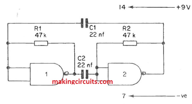
Resistors R1 and R2 are accustomed to bias the inverters as linear amplifiers, and the two capacitors provide the cross coupling.
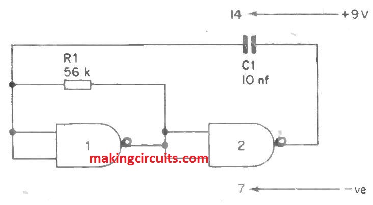
This particular circuit can be simplified somewhat by employing immediate coupling among inverter 1 and inverter 2.
This does away with the requirement for the coupling capacitor which was previously employed in this article, and in addition it obviates the need for the bias resistor for inverter 2

The circuit functions in the subsequent process. Once the supply is initially connected, the output of one gate will go to the high state while the other will go to the low state.
Which of these states the circuit considers is unstable since it is dependent upon the properties of the two gates. With regard to this specific explanation we will assume that inverter 1 has a high output, and inverter 2 has a low output.
C1 will start to charge up from the high output of inverter 1 via R1.
After a period of time which is dependant upon the values provided to R1 and C1, the voltage across C1, and thus also at the input of inverter 1, will reach the transfer voltage of inverter 1.
This particular leads to the output of inverter 1 heading low, and in accomplishing this turns the input of inverter 2 low.
This leads to the formerly low output of inverter 2 to go high.
As this takes place C1 is released into the inverters.
At this point C1 begins to charge up from the negative supply via R1, which is attached to the now low output of inverter 1.
As C1 charges up, the voltage at the inverter 1 will slowly drop, soon after a period dependant upon the time constant of C1 and R1, the transfer voltage of the gate will probably be reached.
This drives the output of inverter 1 high, which often takes the input to inverter 2 high. This leads to the output of inverter 2 to go low, and C1 is again released via the inverters as this all occurs.
The circuit procedure then starts at the beginning again with C1 charging via R1 from the high output of inverter 1. The circuit thus continually oscillates with antiphase squarewave outputs getting developed at the outputs of the inverters.
This particular circuit has numerous benefits over a standard discrete component multivibrator. As we have previously noticed, it has just two frequency.
figuring out parts instead of the regular four. Also it can be made to work over a very vast frequency range. At the low frequency end of the spectrum the main reason for this is the quite high input impedances of the inverters.
This permits quite high values to be used for R1, which when employed in association with a high value for C1 allows an functioning frequency of lower than one cycle per hour to be acquired.
However the circuit will work dependably employing a capacitor of a few pf in value and a resistor of a few K ohms. Operating frequencies into the Meg Hertz region are then possible.
A further benefit of this particular circuit is its low level of current usage. At frequencies within the sound frequency spectrum, or below it, the circuit has a current usage of lower than 500 microamps from a 9 volt supply.
One disadvantage of the circuit is that the frequency of functioning is likely to differ with fluctuations in the supply voltage, and in addition it differs considerably among individual circuits developed to the same design as a result of variations in the transfer voltages of individual inverters. On the other hand, practically in most applications this is of no great importance.
Squarewave Generator
Probably the most preferred use for an astable multivibrator is as the basis of an sound squarewave generator. The circuit diagram of this kind of unit is shown in Figure mentioned below:
This is simply the circuit which was explained in the earlier part, except that the timing capacitor is actually three switched elements, and the timing resistance has been made variable. The three switched capacitors provide the unit with three ranges, the output frequency being variable over these ranges by way of VR1 . The three ranges are the examples below:-
Range 1 20Hz to 200Hz
Range 2 200Hz to 2kHz
Range 3 2kHz to 20kHz
Thus the unit handles the entire sound frequency spectrum. There is really a slight overlap among ranges so that any kind of variations in frequency coverage among individual units should not generate any spaces in the frequency coverage.
As is common to all astable multivibrator circuits, the output waveform of this circuit is not an excellent squarewave, with severe rounding at the top of the leading edge of the waveform.
This is illiminated employing a third inverter as a buffer at the output. The multivibrator chops this from one state to the other with a high quality squarewave being developed at the output. VR2 is the output level control, and the highest peak to peak output voltage of the unit is fractionally less
compared to power supply voltage.

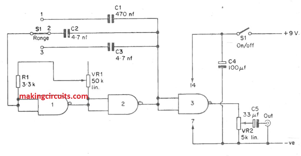
A dial calibrated in frequency can be noted across the control knob of VR1 employing one of the normal techniques for output frequency determination.
Provided C1 to C3 have fairly low tolerances, say 5% or less, a single 20 to 200 scale will suffice for all three ranges (multiply by ten for range 2, and by 100 for range 3).
The pin identification diagram for the 4001 and 4011 devices is demonstrated in below mentioned Fig. These both operate the similar leadout arrangement.


Water Level Alarm
Probably the most common functions of astable multivibrators is in the generation of alarm signals of numerous kinds. The squarewave output is quite strident and is not really effortlessly ignored.
Common CMOS gates find it difficult to deliver adequate output power to effectively drive even a minature loudspeaker, and it is essential to employ a stage of amplification between the output of the tone generator and the loudspeaker.
Figure mentioned below demonstrates the circuit diagram of a water level detector which implements a CMOS multivibrator.
This kind of alarm works extremely well in several applications, for example for keeping track of the water level in the bilges of a boat, and sounding a caution if the level increases above a predetermined point.
They also have household applications, and can be employed as rain alarms, or to signify when the water level in a bath has reached the desired level.
Basically the circuit incorporates an astable driving a standard emitter transistor stage via an inverter/buffer stage. R3 restricts the base current to Tr1 to a safe level.
The loudspeaker forms the collector load for Tr1, and in consequence a significant pulse of current is passed by the speaker each time the output of the inverter/buffer goes high. This causes a loud sound tone to be released from the speaker.
The timing resistor of the multivibrator is not instantly attached between the input and output of inverter 1, but is linked via a sensor. The sensor is an easy device which includes two electrodes which are outlined so that they are bridged by water when it reaches the desired stage (or rain drops fall on the sensor).
The sensor usually acts as an open circuit, and so it does not complete the bias circuit of inverter 1 with the circuit failing to oscillate subsequently.
When the sensor contacts are bridged by the water, the sensor will show a comparatively low impedance as the water will deliver a conductive path amongst the two electrodes.
This finishes the bias circuit and the alarm will sound, and will pursue to do so provided that power is placed on the circuit and the sensors electrodes are bridged by water.
It is worth observing that even though pure water is a bad conductor of electricity, rain, tap, and sea water consist of adequate impurities to generate a low impedance path amongst the electrodes.
R2 is essential for two factors. First of all, it is not a good idea to leave an inverter's input open circuit, as would normally become the situation in this article when the alarm is not sounding.
Due to the fact it will usually acquire stray disturbance which would produce a constant noise to be comprised from the speaker. It would also lead to wasted power.
The second thing is, this resistor guarantees that when the alarm is not functioning, no current flows through the speaker. By taking the input of inverter 1 high under static situations R2 shows that the output of inverter 3 is low, and Tr1 is cut off.
If the circuit was to latch in the reverse state (inverter 3 output high) a substantial quiescent output current would probably flow.

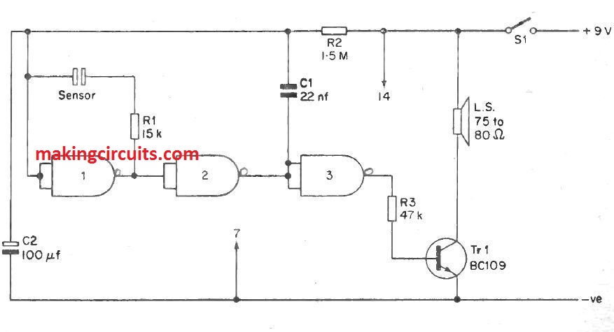
The circuit incorporates a idle current usage of merely a minute fraction of a micro amp, and you can easily power the circuit from a battery even if it is to be used for very long periods. The current consumption when the alarm is functioning is something in the region of 18 mA.
Unless the leads to the sensor are remarkably long, or pass close to a mains lead or some similar source of electrical interference, it is not necessary for them to be screened. If this cable does need to be of the screened variety, a single screened sort can be employed (outer to R1, inner to inverter 1 input).
Christmas Tree Lights Flasher
Numerous beneficial gadgets can be designed employing a multivibrator to drive a relay, and a famous example is a Christmas Tree Lights Flasher. This will offer a much more standard flashing rate than can be acquired simply by using a bimetal sort flashing bulb, and the flashing rate can also be designed variable. The circuit diagram of this device presents itself in below mentioned Fig.

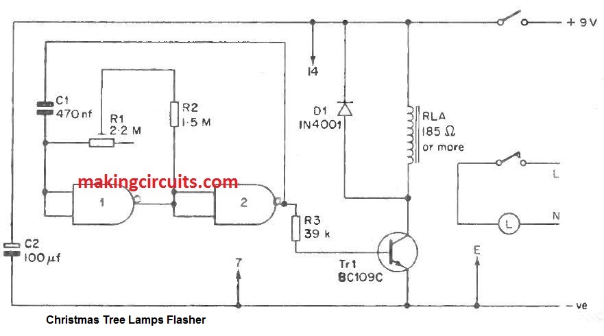
The two inverters are linked as a low frequency astable circuit, and the functioning frequency of this is variable over a range of about 0.5 to 1.5 Hz via R1. The output of inverter 2 drives common emitter amplifier Tr2, via R3. R3 is a current limiting resistor.
Tr1 has the relay coil as its collector load, and the relay will be energized when the output of inverter 2 is high. The relay will be off when
the output of inverter 2 is low. A single set of relay contacts (either normally closed or normally open ones) are accustomed to manage the lights.These will as a result turn on and off at a rate dependant upon the setting of R1.
D1 is a protective diode, and this is required to take care of the circuit against the high reverse voltage which is designed across the relay coil as the power to the circuit is turned off.
This voltage is created by the magnetic lines of force instantly decaying and cutting through the relay coil.
As a result of speed at which this magnetic force dies away, quite a high voltage can be generated, but it is at a high impedance. D1, simply, shorts out this voltage, and is guarded against passing an extreme current by the high source resistance of the signal.
D1 should not be avoided from the circuit as this voltage spike is fairly capable of destroying both the I.C. and Tr1.
Metronome
A low frequency astable multivibrator can be employed as the basis of a very simple metronome, and the circuit diagram of such a metronome is found in below mentioned Fig.

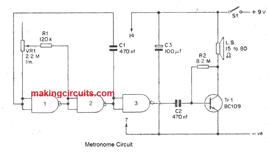
Inverters 1 and 2 widely-used to form the astable circuit, which has a continuously variable frequency range of roughly 0.5 to 511z.
The frequency is modified by way of VR1.
The output of the multivibrator is fed to an inverter/buffer stage, and the output of this drives a single transistor output stage. R2 is the base bias resistor for the output transistor (Tr1), but this has a very high value and it does not bias Tr1 into class A function. It only takes Tr1 just further than the threshold of conduction, and this stage produces results in the class B mode.
When the output of inverter 3 goes positive, a brief positive pulse is fed to the base of Tr1 signifies C2, and this turns Tr1 hard on throughout the pulse.
This causes a quick but relatively large pulse of current to be passed by the speaker which forms the collector load for Tr1. C2 has deliberately been given a fairly low value so that the duration of this pulse is short, and a click of a fairly high pitch is produced from the speaker.
This makes a very good simulation of the click generated by a normal metronome. Of course, a click is generated each time the output of inverter 3 goes high, and this triggers about 40 to 300 clicks being generated each minute, the desired rate being set by using VR1. A beat rate of 40 to 300 per minute covers all normal musical specifications.
When the output of inverter goes negative, no substantial sound output is developed. The reason being the output transistor will be cut off by the negative voltage pulse which is delivered to its base. Being biased into class B function, Tr1 is practically cut off anyway, and the negative pulses as a result have no actual impact on the output stage.
This provides the unit a very low average current consumption, and the current consumption of the prototype is only about 2 mA.
A dial calibrated in beats per minute ought to be noted across the control knob of VR1, and this is pretty easy to execute. The range of functioning frequencies is so low that it is really simple to count the number of beats per minute generated with VR1 at different settings.
The dial is then calibrated at these settings.
It is important to search for settings that correspond to beat rates that are divisible by five or ten, as a dial calibrated at points such as 40, 70,
100, 150 etc., will appear far more organized than one calibrated at points such as 42, 71, 98, 153 etc.
The fact is that, the only method to discover the preferred calibration points is by experimentation, and this is likely to be time consuming.
It is possible to save a certain amount of time by counting the number of beats in a 15 second period and then multiplying this by four to find the numbers of beats per minute, instead of using a straight forward minute count.
This should not be completed at the lower calibration points because precision could suffer resulting from this.
Transistor Tester
The majority of transistor testers are developed to test a transistor which has been removed from its circuit, or to test it prior to being attached into circuit.
Provided one does not need to really measure the gain or some other parameter of the device under test, most commonly it is pretty feasible to test the device while it is attached into circuit. The circuit diagram of such a 'Go' - 'No Go' tester is demonstrated in blow mentioned Fig.

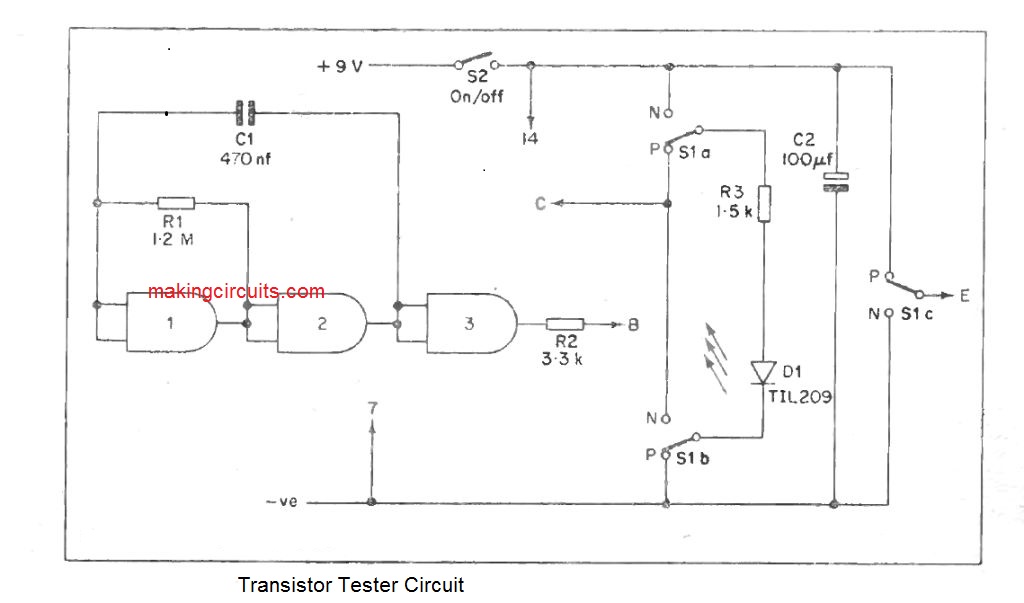
The concept of this circuit is merely to apply a periodic forward bias to the base of the transistor while supervising its collector current.
The bias signal is extracted from the output of an inverter which is driven from a low speed astable circuit. The collector current is examined by a light emitting diode indicator (D1).
If we look at the circuit first in the p.n.p. screening mode. When the output of the inverter is high, the base of the transistor will be at virtually the same potential as its emitter, and it will as a result not perform. The L.E.D. will not illuminate mainly because it will receive no substantial current.
As soon as the output of inverter 3 goes low, a large forward bias is put around the test transistor which should, in consequence, be biased into saturation. A large current will flow via D1 which will illuminate.
Thus if the transistor under test is a good functional device, upon linking the test prods to it, the L.E.D. indicator should flash ON and OFF (at a rate of around 1 Hz).
If the test transistor is a closed circuit device, then obviously the bias will have no impact, and D1 will be on constantly. If the transistor is an open circuit device, then D1 will not turn on at all.
The circuit functions in exactly a similar way when it is turned to the n.p.n. mode, apart from the transistor is shut down when the output of inverter 3 is low, and saturated when it is high. The unit is employed in a similar way no matter which mode it functions.
It should probably be noticed that this circuit is not fool proof, and it can give deceptive outcomes. The reason being the base and emitter of the test transistor aren't actually short circuited jointly once the device is designed to to be cut off.
Hence, it is merely possible that circuit resistances could bias the transistor on. It is also feasible that circuit resistances could supply a path for the L.E.D. current flow. Thus the L.E.D. could possibly be continually on even though the test transistor is sound.
Additionally it is possible that the L.E.D. could fail to come on even if the transistor is functional. This could happen if it has a low resistance in its base - emitter circuit, as the potential divider impact among this and R2 of the tester could develop a base - emitter voltage of inadequate level to switch the transistor on.
Benefits acquired with this particular tester should not, as a result, be considered as being infallible. When testing ordinary low level transistor stages the device is impossible to generate incorrect results, since the required low circuit resistances won't be present. Extreme care ought to be practiced when testing power devices though.
It can be stated in favour of this tester that its performance is disproportion-ate to its really low price.One last point is that no power should be attached to the circuit in which the test transistor is utilized.
Low Power Pilot Light
It is important to fit a pilot light to any item of electronic equipment, such as signal generators, and electronic voltmeters, where it is possible to accidentally leave the equipment turned on. This is particularly so when it comes to battery operated equipment, where leaving the equipment switched on will end up being somewhat costly.
Fitting a pilot light to battery operated equipment does signify something of a difficulty since in order to be beneficial, the pilot light must consume very little battery current. Or else it could properly consume more power than is stored by always keeping in mind to turn the devices off.
Light emitting diodes will provide visible light from quite low operating currents, but in order to provide an extremely noticeable light level they actually ought to consume something around 10 mA. This is more than is consumed by many pieces of battery controlled devices.
The best way of decreasing the current usage of an L.E.D. pilot light is to use a pulsing method. For instance, if during one second periods the L.E.D. is only briefly switched on for (say) 0.1 seconds, then the average current consumption will probably be decreased by 90%.
In this manner the L.E.D. can be designed to develop a very apparent pilot light with a current consumption of only 1 mA or even less.
Additionally, the point that the light is flashing will tend to make it more apparent than one which is on continuously. Hence, even though it employs less power, a flashing pilot light much more effective.
The low current consumption of a CMOS I.C. causes it to be the best basis for a low power pilot light, and the circuit diagram of this kind of unit seems in Fig mentioned below. Inverters 1 and 2 are employed as an astable multivibrator, and inverter 3 is employed as a buffer stage which operates the L.E.D. indicator.

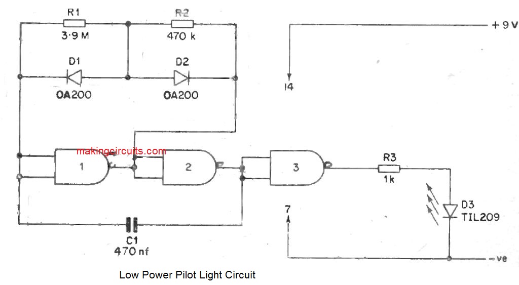
It will likely be viewed through Figure mentioned above that this astable circuit is a improved version of the type employed in the prior circuits. The timing resistor has been split up into two different components (R1 and R2), and steering diodes are already included (D1 and D2).
In effect, these types of diodes short out one resistor when C1 is charging through the positive supply, and the other resistor when it is charging from the negative supply. It charges from the positive supply via R1, and through the negative supply by means of R2.
As R1 has a higher value than R2, the output of inverter 2 is in the high state longer than it is in the low state. This must be scenario since it will require the voltage across C1 longer to achieve the transfer voltage of inverter 1 when C1 is charging through the higher resistance.
An inverter in interposed amongst the output of inverter 2 and the L.E.D. circuit, and so the voltage at this point is low for longer periods than it is high. The circuit functions at a frequency of around 1 Hz, and so D1 is quickly turned on at around 1 second time frames.
The average current usage of the prototype circuit was measured at about 900 micro -amps from a 9 volt supply.
0-10 Second Timer
This is a easy device which generates an sound tone soon after a switch is controlled. The delay is variable from zero to about ten seconds. Simple timers similar to this can be utilized in T.V. sort quiz games that result in a time limit during which the query can be solved if one is to score.
They are able to also be used in other games, like lightning chess or droughts, and there must be a number of other achievable purposes of this kind of devices.
The circuit diagram of the timer is demonstrated in below mentioned Figure. Inverters 1 and 2 are employed as a self-explanatory sound frequency astable circuit which really functions at a frequency of around 500 Hz.


The output of the astable is fed to a usual emitter amplifier by using a pulse enabling circuit. This simply includes among the NAND gates of a 4011 1.C., and the method by which this functions is very easy.
Once the control input of the gate is in the low state, input indicates at the signal input may have no impact on the output. The reason being the output of a NAND gate is higher except if both the inputs are high, whereby the output occupies the low state.Therefore if the control input is low, the state of the signal input is unnecessary as the output will be high.
As a result, when the control input of gate 3 is low, its output is going to be high and Tr1 will probably be cut off. No sound will be produced from the speaker.
When S1 is opened, the voltage at the control input of gate 3 will start to rise as C3 charges up through VR1 .When the voltage across C3 will go over a transfer voltage of the enabling gate, the output state of this gate will be based mostly on the signal at its other input.
Once the signal input is low the output is high, and the output is low when the signal input is high. Tr1 will then be pulsed ON and OFF and an sound tone will probably be designed from the speaker.
The time consumed for the voltage around C3 to reach the transfer voltage of gate 3 is dependent upon the setting of VR1 . When this is modified for zero resistance there is certainly zero delay.
This could be increased to a optimum delay of around ten seconds with VR1 at maximum resistance. Be aware, on the other hand, that the maximum time delay will be different relatively between individual circuits as a result of wide tolerances of particular elements (C3 specifically).
The circuit is reset by closing S1 which in turn discharges C3 and therefore cuts off the sound tone. A new timing period is commenced by beginning S1 again.
A 4001 I.C. is not appropriate for use in this particular circuit considering that gate 3 is not employed as an inverter, and the NOR gates of a 4001 may not supply the desired circuit activity.
However in this particular circuit description the inputs of gate 3 were known as the signal and control gates, the inputs to this gate can be linked either way round. Whichever one is attached to C3 turns into the control input and the one linking to gate 2 turns into the signal input.
Pulsed Tone Generator
Two circuits employing audible alarms have been explained up to now, these types of both work with easy constant tone circuits. A more efficient alarm could be generated by either possessing a tone of different pitch (for example police car sirens), or by employing an intermittent tone (as do many burglar alarm systems as an example). The circuit demonstrated in below mentioned Fig. is of the second option sort.

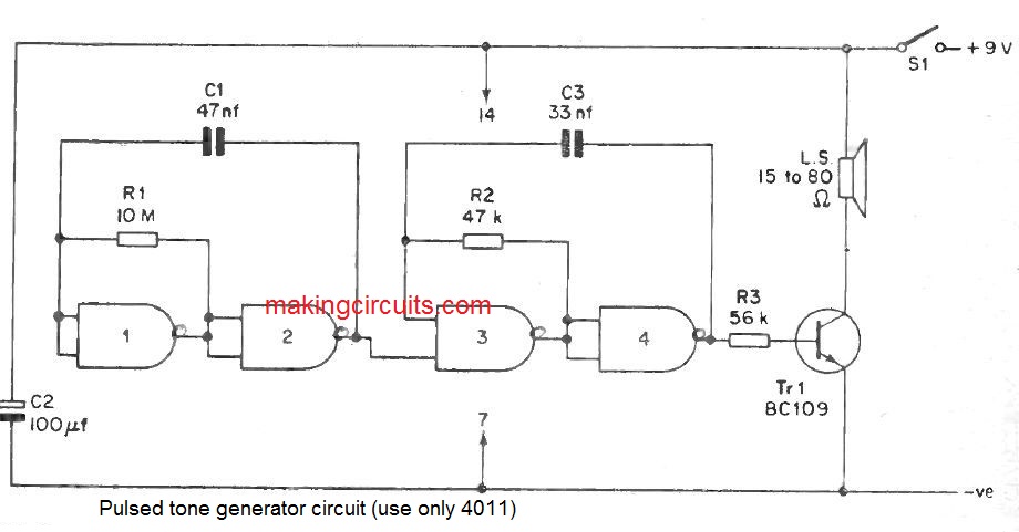
In this article inverters 1 and 2 form a low frequency astable possessing an functioning frequency of around 1 Hz, and inverters 3 and 4 are employed as an astable tone generator functioning at a frequency of around 800 Hz.
Gate 3 is not utilised as a simple inverter, however is employed as an enabling gate.
When the output of the L.F. astable is lower, the tone generator will certainly be blocked and will be struggling to oscillate. When output of the L.F. astable is higher, gate 3 will work as a common inverter and the tone generator will operate normally. Hence the low frequency astable switches the tone generator ON and OFF at a rate of around 1 Hz, and an intermittent output is developed.
Gate 3 is employed as the control gate instead of gate 4, as with the option process the output of the tone generator would be high when the circuit is at the muted state. This could switch Tr1 on as well as would certainly result in increased current usage.
Pulsed Output Timer
This is a uncomplicated topic to modify the pulsed tone generator circuit to generate a easy timer of the type explained previously, however a pulsed output obviously. The circuit diagram of this device presents itself in Figure.

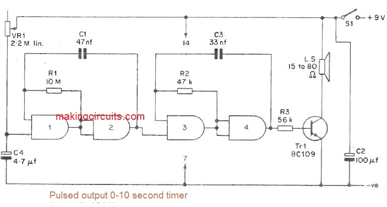
In this article gate 1 is employed as an enabling gate, and the control input is generally held in the low state by S1. This stops the low frequency astable from oscillating, to result in its output to be in the low state. This leads to the tone generator astable to also generally be blocked, and so no output is produced from the speaker.
When S1 is opened, C4 starts to charge up via VR1, and when the potential across C4 exceeds the transfer voltage of gate 1, the low frequency astable will switch on. The pulsed tone generator then performs usually with an intermittent tone being released from the speaker.
BISTABLE CIRCUITS
The bistable is the easiest of the multivibrator family, however it is not really employed almost although the astable type. As a matter of fact it is not often encountered in circuits for the amateur, however it can be extremely beneficial on events.
A bistable can be quite effortlessly created from quite a number of CMOS inverters, and only two resistors and two push button switches are essential besides the inverters. The circuit diagram of a simple CMOS inverter is demonstrated in figure mentioned below.

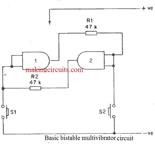
In this particular kind of circuit one output is low and the other is high. The circuit as a result has two stable states, and it is using this that it introduced its identity.
Which output goes high and which goes low when the power is at first attached to the circuit is dependent upon unpredictable parameters. It is primarily based upon the functioning speeds of the inverters. Suppose for instance, that inverter 1 has the ability of quicker function than inverter 2.
When the supply is switched on, the inputs of both inverters will probably be low, and the outputs will attempt to go high. The output of inverter 1 will go high at a faster rate than the output of inverter 2, and a increasing voltage will as a result be connected from the output of inverter 1 to the input of inverter 2 via R1.
This voltage may have the result of holding inverter 2 output in the low state while the output of inverter 1 goes high. The circuit then rests in this state.
The circuit can be designed to occupy the opposite state by momentarily functioning push button switch S2. This takes the input of inverter 2 low and its output to go high. This takes the input of inverter 1 high as this particular is attached to the output of inverter 2 via R2. In consequence the output of inverter 1 goes high.
Even though S2 is released, the circuit will continue to be in its new state. It can be delivered to its original state by functioning S1 momentarily.
This particular circuit creates a kind of simple electronic memory, due to the fact as soon as it is placed in a specific state it continues to be in that state, and could be considered to remember that state. It is also quite often termed as a latch, considering that once set in a particular state it latches in that state.
Switch Precedence Indicator
One famous usage of bistable circuits is in switch precedence indicators. This is actually the kind of device which is often used in T.V. sort quizzes where the first person to press his or her switch has the first chance to reply to the questions. The objective of the device is to provide the unoperated switches inoperative the moment one of the switches is shut.
Similar games are usually performed in the home, and such a device works extremely well when playing games such as snap, the popular card game.
The circuit diagram of a simple switch precedence indicator is demonstrated in the Fig mentioned below.

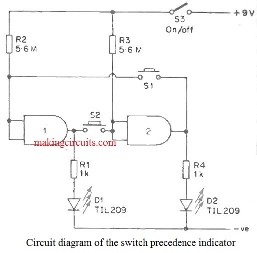
Both lamps are off when neither of the switches are turned off, considering that the input of each inverter will probably be taken high by its bias resistor (R2 and R3). The output of each inverter will as a result be low, and neither L.E.D. indicator will probably be provided with any current.
If one of the push button switches is operated, say S1, then the suitable indicator lamp will turn on. In this instance it will likely be D1 which will switch on, as the input of inverter 1 will be taken low by being attached to the low output of inverter 2.
If S2 is now operated, D2 will not switch on because the output of inverter 1 is high, and closing S2 will simply keep inverter 1 input in its present state. Therefore when a push button is operated the appropriate lamp will turn on, and the other push button is blocked, and will have no impact on the circuit.
The circuit is reset looking forward to a new round to start off by simply releasing the push buttons.
This particular circuit, along with the simple timer explained previously, might form the basis of a easy reaction testing game. The timer will be set to provide a delay of a few seconds and then it would be commenced.
The two players would each have a push button switch, and the winner will be the person who operated his or her switch the most swiftly as soon as the audible alarm had commenced to sound.
Heads Or Tails Simulator
Yet another well-known kind of novelty circuit which regularly implements a bistable circuit in certain form or other is a heads or tails simulator. This sort of circuit is designed to electronically simulate the tossing of a coin. The circuit diagram of such a device is mentioned below:-


Inverters 1 and 2 are linked as an astable circuit possessing an functioning frequency of a few hundred Hz. The other two inverters are attached as a simple bistable circuit.
The simplification is just that inverter 3 output and inverter 4 input are instantly linked with each other, instead of being linked by using a resistor. This is feasible as no input signal is placed on the input of inverter 4.
The input signal is coupled to the input of inverter 3 from the output of the astable circuit via S1. When the power is switched on the input of the bistable will probably be quickly switched through the high to the low state by the astable multivibrator.
The input and output of the bistable are in phase, and so the output will also be quickly heading from the high to the low state. Each time the output goes to the high state, D1 will quickly be pulsed on.
It will be flashing on and off at such a fast rate though, that to a human observer the flashing will not be perceivable, and the lamp will appear to glow constantly.
When S1 is opened, the bistable will latch in whatever state it was in at the instant S1 broke the continuity of the circuit. For example, if the output of the bistable was in the high state when this took place, its input will be held in the high position by the voltage which is coupled from output to input by R2. The L.E.D. indicator will as a result continue to be on.
The input of the bistable will in the same way be held in the low state by this coupling if the output happened to be low at the instant S1 went open circuit, and in result the L.E.D. would go off.
The output from the astable circuit is a squarewave, and so the bistable is driven to the high and low states for equal lengths of time. It is therefore solely a matter of chance whether the indicator lamp continues to be on or switches off when S1 is operated. There is a 50-50 chance of it assuming any one of the two possible states, in the same way you can find when one tosses a coin.
By classing the on state of the lamp 'heads', and the off state 'tails', the unit will hence replicate the tossing of a coin. Unlike some other heads or tails circuits, this method needs no modification or testing with circuit values in an effort to achieve appropriate 50-50 function.
Simple Touch Switch
Touch switches appear to have grown to be very popular nowadays, and even though this might be generally because of their unique value instead of any kind of practical benefit, they do possess specific practical advantages over more conventional forms of switch.
Most likely the major one in most applications is that they can be made to have no moving parts to wear out. This tends to make them as efficient and hard wearing as the main (electronic) part of the equipment they are controlling.
The circuit diagram of a simple touch switch employing a CMOS bistable circuit is demonstrated in below digram. This will likely deliver ON/OFF switching for any piece of 9 volt battery operated equipment which does not have a current usage of more than 100 mA (the utmost functioning current for the BC179 transistor).

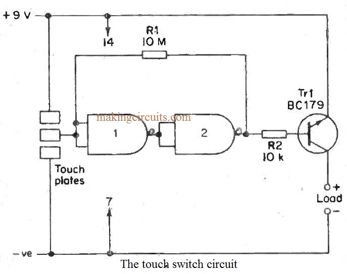
CMOS 1.C.s are perfect for use in this specific application simply because they can merely supply the required extremely high input impedances, and they also consume no substantial current when they are not generating a load.
The current usage of this circuit in the off state is very low, being actually lower than 1 micro -amp. There is certainly eventually no significant battery drain when the equipment is switched off, and the the circuit diagram of a simple touch switch employing a CMOS bistable circuit is displayed in the above touch switch circuit diagram..
This will likely deliver ON/OFF switching for any piece of 9 volt battery operated equipment which does not have a current usage of greater than 100 mA (the maximum operating current for the BC179 transistor).
CMOS 1.C.s are perfect for easy use in this specific application simply because they can certainly supply the required higher input impedances, and in addition they also consume no substantial current when they are not generating a load.
The current consumption of this circuit in the off state is extremely low, being in fact lower than 1 micro -amp. There is certainly consequently no significant battery drain when the equipment is switched off, and the battery life ought not to be drastically lower than if a mechanical switch were employed.
Extra current is consumed when the unit is in the on state, this primarily being the base current to start up Tr1. This really is unavoidable, however the additional current consumed is less than 1 mA, and is likely to be of no importance in the most of applications.
The circuit functions in the subsequent method. When the power is at first attached to the device the output of the bistable will go into the higher situation. Tr1 is shut down and no power is employed to the load.
It is easy to alter the state of the bistable by touching the lower set of touch contacts. The resistance of the operators skin then takes the input of the bistable low, and the output of the bistable will then also go low. A base current is then placed on Tr1 which is biased into saturation, and virtually the full supply rail potential is delivered to the load.
The unit can be turned off again by touching the upper set of touch contacts. The input of the bistable is then attached to the positive supply by way of the skin resistance of the operator's finger, and in result both the input and output of the bistable occupy the high condition. Tr1 is as a result cut off yet again, with no substantial current being delivered to the load.
R1 supplies the required latching action by holding the input in what-ever state it was in once the finger of the user is eradicated through the touch contacts. If required, the sensitivity of the circuit could be enhanced by increasing the value of R1.
Resistors possessing values of more than 10 Megohms aren't easily accessible, and so an increased value for R1 can only be acquired by adding two of more resistors in series to generate up the essential value.
R2 is required to be able to avoid Tr1 from passing an extreme base current. It also restricts this current to an efficient level. If the unit is being employed to control a fairly high current load, say 25 mA or more, it is essential to lessen the value of R2 to 1 k.
With a little ingenuity it will not be too tough for the constructor to fabricate appropriate touch contacts. A piece of stripboard can be employed to produce a quite simple but efficient touch plate, or an even better one can be etched from a piece of copper laminate board.
Even three screws (Pan or Countersunk heads) installed on the front panel of the main equipment could be employed if they are proper placed.
Relay Operated Touch Switch
In certain applications the above mentioned circuit will not be appropriate mainly because it will simply control 9 volt equipment which includes a current consumption of 100 mA or less. If one desires to control a higher power, or an alternating current, this could be achieved by controlling the load by using a relay possessing appropriate contacts.
In this manner additionally it is possible to possess change over switching, and such things as touch controlled wavechange switches turn into a opportunity.
The circuit diagram of the relay version of the touch switch seems in Figure below. This is actually the similar to the original circuit except that Tr1 at this point have a relay as its collector load instead of the controlled equipment.
Protective diode, D1, has also been included.


The relay can be any type which is appropriate for 6 volt operation and has a coil resistance of 185 ohms or more, provided it has appropriate contacts for its meant application, certainly.
MONOSTABLE CIRCUITS
It is most likely true to confess monostable circuits are one of the minimum used of most electronic building blocks, in terms of circuits for the amateur are concerned anyhow.
They are possibly employed more regularly at this point than they were a few years ago as monostable I.C.s such as the NE555 and 74121 have turned out to be very functional.
CMOS monostable devices are accessible, and an example is the 4047 I.C. On the other hand, when merely a easy monostable is needed it is almost always simpler and less expensive to connect a couple of gates to form a monostable circuit.
A simple monostable can be created from an inverter and a 2 input NOR gate. Hence , it is possible to create one (or two) from a 4001 I.C. The relevant circuit diagram is shown below.

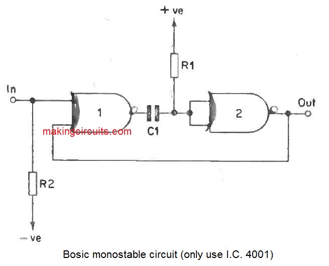
The input of the inverter (gate 2) goes low when the power is at first attached to the circuit. The reason being its input is taken high by R1. The output of gate 1 may also be high since both the inputs are low. If either or both of the inputs of a NOR gate go high, the output will go low.
If a brief pulse is placed on the input of the circuit, this will likely momentarily take one input high and gate 1 output will as a result go low. This output pulse is fed by way of C1 to the input of the inverter, and in result the output of the monostable goes into the high state. This takes the second input of gate 1 high, and even if the other input now goes low, the output of gate 1 will continue to be in the high state.
C1 will start to charge up via R1 as soon as the output of gate 1 goes low, and finally the voltage on C1 will reach the transfer voltage of gate 2, and its output will go low.
This takes the second input of gate 1 low, and the circuit has now arrived to its original and only stable state. It is out of this that the label monostable has been derived from.
It is really worth noticing that even if the input to the circuit is taken positive for a long period, rather than just momentarily, the output waveform is definitely the similar. This simply has the effect of holding the output of gate 1 low if a positive input continues to show at the end of the output pulse. When this input is at some point taken out, then the circuit returns to its original state.
Hence a monostable multivibrator can easily be employed to either lengthen a brief input pulse or shorten a long pulse. The length of the output pulse is regulated through the values directed at C1 and R1.
The length of the output pulse could be varied over very wide limits as it can be less than a micro -second to more than an hour. R1 may have a value of any-where between 10 k and many Megohms. C1 can be any value of more than a few pF. If C1 is an electrolytic type it has its positive terminal linked to R1.
With R1 at a value of 1.8 Meg the prototype gave an output pulse of around 1 second per infd, but there is probably afairly large variation amongst individual circuits in this respect. This is regarding the main drawback to this particular quite simple circuit.
Capacitance Meter Circuit
The majority of multimeters are equipped to measure wide ranges of voltage, current, and resistance, but couple of, if any, are designed for capacitance measurements.
Because of this, the majority of electronics lovers are not able to carry out capacitance measurements, and this must lead to many useable capacitors being extracted mainly because their identification markings are getting to be wiped out. Some ways of testing capacitors is also very beneficial when one is employed on providing defective equipment.
A capacitance meter is as a result an extremely beneficial piece of equipment to have in the workshop. A simple capacitance meter can be based on an astable and a monostable multivibrator, and it is feasible to create one employing a single CMOS IC. as the only effective device. The circuit diagram of this type of unit is demonstrated below; and this works with a single 4001 IC.


Gates 1 and 2 are linked as the astable circuit and gates 3 and 4 form the monostable multivibrator. The astable functions at a frequency of approximately 100 Hz, and its output is fed to the activate input of the monostable.
Therefore one hundred times per second the monostable will develop an output pulse. The length of this output pulse is dependant upon the values of the timing components, and the timing capacitor under test. The timing resistor is probably the four resistors, R3 to R6, and is whichever one is switched into circuit by S1.
By employing four timing resistors the unit is capable of providing four measuring ranges. However these are the examples below:-
Range 1 0 to 500 nF
Range 2 0 to 50 nF
Range 3 0 to 5 nF
Range 4 0 to 500 pF
The unit therefore consists of most conventional amateur needs.
The circuit value happen to be selected in order that the monostable functions as a pulse shortener. As an example, with the unit turned to Range 1 and a 500 nF test capacitor in circuit, the output pulse through the monostable will undoubtedly be about half the length of the trigger pulse from the astable. Lower values of test capacitance will certainly generate a much shorter monostable pulse length.
A voltmeter circuit composed of M1 and one of the set of four preset resistors (R8 to R11) is linked at the output of the monostable. Every time the output of the monostable goes higher, a pulse of current will probably be fed to the meter.
A constant string of pulses are produced when a test capacitor is attached to the unit, and the meter will react to the average output voltage.
With a 500 nF test capacitor in circuit, R9 is modified to generate f.s.d. of the meter. If, for example, a 100 nF capacitor is attached instead of the 500 nF one, the length of the output pulses will simply be one - fifth of the earlier duration.
The rate where the monostable is activated is the similar, therefore, the pulses continue to take place at the same frequency. Hence the average voltage throughout the meter circuit will simply be one -fifth of its original level, and the meter will read one -fifth f.s.d.
It will probably be obvious because of this that there is a linear relationship amongst the meter reading and the value of the test capacitor. The unit hence performs quite successfully as a linear reading capacitance meter.
On Range 2 the timing resistor is ten times the value of that utilized on Range 1. Only one -tenth of the earlier test potential is as a result required to generate equivalent meter reading. For instance, 500 nF was required to generate f.s.d. of the meter on Range 1 although merely 50 nF will probably be required on Range 2.
In fact this is simply not quite the situation considering that the tolerances of the timing resistors avoid such a accurate relationship from being gathered. In an effort to make certain that good consistency is gathered on all four ranges, an alternative preset resistor for every range is made available in the meter circuit. This permits each range to be calibrated towards a close tolerance capacitor.
A different option technique is to apply 1% tolerance components for R3 to R6, and a single calibration preset. The unit would certainly then only need to be calibrated on one range, with good consistency being immediately acquired on the other three ranges.
D1 and R12 widely-used to stablise the supply voltage of the circuit, and this is really important if steady and trustworthy outcome is received. There are actually two advantages for this particular. First of all, the frequency of the astable circuit will change somewhat with modifications in supply rail potential.
If it should speed up at all, then there will be more pulses placed on the meter in a presented time frame, and increased meter readings will probably be acquired. If the speed of the astable ought to reduce, then certainly all meter readings will probably be low.
Second of all, the more importantly, the output voltage pulses of the monostable are almost similar in amplitude to the supply rail voltage. If the supply rail alters (because of battery ageing for instance), then the meter readings will alter proportionately.
An easy battery check facility is integrated in the circuit, and this simply includes S2 and R7. When S2 is in the position displayed, the circuit operates normally. The meter is linked throughout the stabilised supply rail when S2 is in the other position.
It is attached by way of R2 which changes the meter into a 0 to 10 V voltmeter. This is often employed to observe the supply potential, and when it drops below its nominal level of 7.5 V, this suggests that a new battery is essential.
Calibrating the unit is pretty uncomplicated, and four close tolerance capacitors are essential for this. For instance, a 470 nF 2% capacitor could possibly be employed to adjust Range 1. With this connected over the test terminals and the unit set for standard function on Range 1, R10 would be modified for a reading of 47 on the meter.
It is advisable not to utilize a calibration capacitor that includes a value corresponding to less than half f.s.d. of the range being calibrated, as this may lead to inferior accuracy being acquired. It is preferable in the beginning modify all the preset resistors for maximum resistance just before starting calibration of the unit.
Simple Timer Circuit
Probably the most apparent use for a monostable is as an easy timer.
This sort of circuit is designed for this application, and the circuit diagram of a easy enlarger timer possessing a CMOS monostable is displayed in
below diagram. This has a timing period which is constantly variable from about 1 second to 2 minutes.

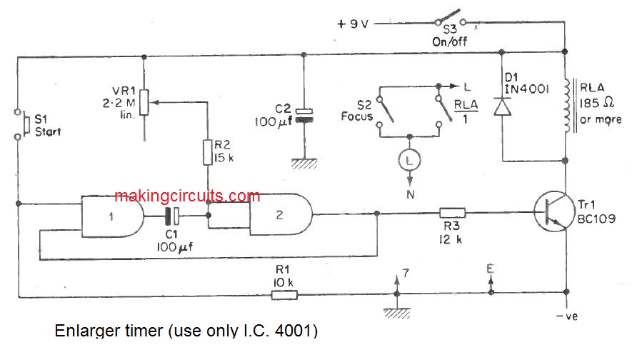
The two gates are attached as a uncomplicated monostable which is often physically triggered by using push button switch S1. VR 1 allows the timing resistance to be varied on a wide range of values, and this permits the specified timing period to be fixed.
Tr1 is usually turn off however it is turned hard on when the output of the monostable goes high. In doing so it energies the relay coil, and the usually open contacts of the relay connect the power to the enlarger lamp.
Obviously, at the conclusion of the timing period the output of the monostable will go low and the enlarger lamp is switched off. D1 is the regular protecting diode.
S2 permits the enlarger lamp to be switched on independently of the tinting circuit, and this is a beneficial function with regards to the focusing of the enlarger.
C1 must be a superior quality component possessing a low leakage current if trustworthy and constant benefits can absolutely be acquired.
It is essential to mark a dial around the control knob of VR 1, and this should if possible be calibrated at one second time intervals. Tagging this out is pretty time consuming because the only solution to obtain the calibration points is by using trial and error.
Peak Level Indicator
A peak level indicator is a device which will provide a warning of an over-load in an amplifier, tape recorder, mixer, or any other part of sound objects. Contrary to the typical average reading VU meter, this sort of indicator has a very quick answer and it will interact to even very brief transients as it is controlled by peak instead of average or R.M.S. levels.
It should be emphasised that a peak level indicator is not supposed to have been employed rather than VU meter, but will probably be employed in conjunction with one. A single peak level indicator will simply display when an over-load has taken place. It will not display, the signal level.
The circuit diagram of a peak level indicator which uses a CMOS monostable is displayed in Figure below. Gates 2 and 3 form the monostable, and the output of this is employed to drive L.E.D. indicator D1 via current restricting resistor R6. The L.E.D. indicator will turn on when the output of the monostable goes positive. The circuit values happen to be selected to generate an output pulse of around 0.2 seconds in timeframe.

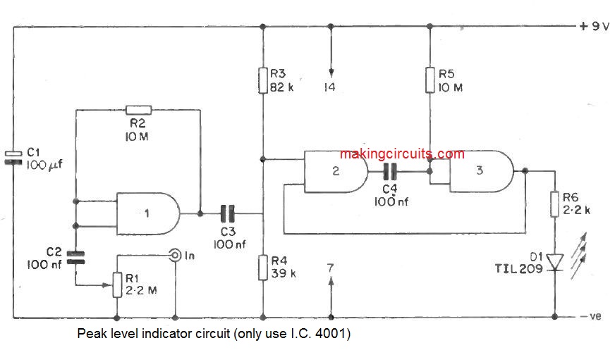
R3 and R4 are accustomed to bias the input of the monostable towards its trigger voltage, but the voltage generated by this potential divider is not enough to really activate the circuit. The real reason for employing this network is that it decreases the peak input voltage which can be needed in an effort to trigger the monostable, and it therefore enhances the tenderness of the circuit.
It does not enhance the sensitivity pretty enough to allow the unit to be used which includes parts of devices, and so an amplifier stage continues to be incorporated prior to the monostable. This is based on gate 1, and the access to the CMOS gates as linear amplifiers will be taken care of completely later on. R1 is a sensitivity control, and this permits the unit to be modified to reply to any input signal level of around 500 mV peak to-. peak or even more.
The amplified input signal will modulate the voltage at the input of the monostable, and when a positive peak takes the input above the transfer voltage of the gate the monostable will be activated. This will likely result in
D1 to be quickly pulsed on.
It is an important function of the circuit that it must be the peak level of the signal which the circuit reacts to, the input waveshape and its mean level being not important. To be able to acquire constant function using this circuit it is essential to power it from a stabilised supply.
An input for the unit is obtained from any appropriate point in the VU meter circuit, and as the unit has an input impedance of around 2 Megohms it will not considerably load the VU meter circuit.
For this reason very high input impedance it might be useful to employ screened input cable, even though this will likely not be essential if the unit is fed from a pretty low source impedance.
R1 is altered in the subsequent method. Link a sinewave generator to the input of the main equipment and adjust the controls to signify the essential overload level on the VU meter (generally either +3 or +6 dB). Alter R1 for the lowest sensitivity which in turn causes the L.E.D. indicator to be continuously on.
Stereo Version Indicator
For stereo function it is feasible to utilize two of these peak level indicators, one to monitor each channel. It is far more convenient on the other hand, to employ a circuit which uses one indicator lamp for both channels. This is often achieved by providing the outputs of two of the circuits explained above to the circuit demonstrated in below diagram. R6 and D1 of each of the original circuits are removed, and the current circuit is fed direct from the outputs of the monostables.

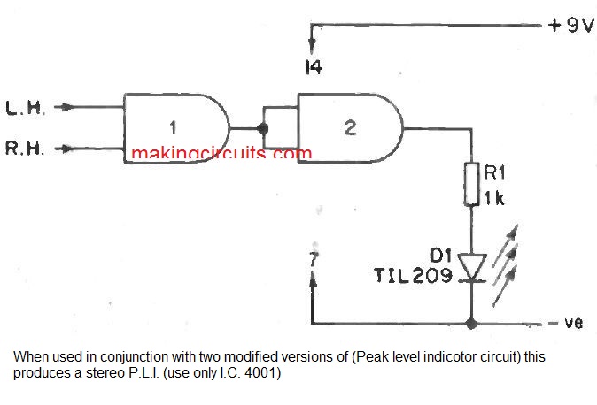
In this article a NOR gate and an inverter are attached to form an OR gate.
When both the inputs to gate 1 are in the low state, its output will be high.
The output of the inverter will as a result be low and D1 will not illuminate. If either or both the inputs to the NOR gate go high, then its output will go low. This will lead to the output of the inverter to go high and D1 will probably be switched on.
The circuit in general (for example the two monostables) will as a result trigger the indicator lamp to come on if the peak level threshold of either channel is surpassed.