


In this post we learn how to simple oscillator circuits using CMOS NAND gates. We comprehensively learn many typical oscillator circuits such as,
- Crystal Oscillator Circuit
- Pierce Oscillator
- L-C Oscillator
- Hartley Oscillator
- Phase-Shift Oscillator
Let's begin the tutorial:
Crystal Oscillator
Crystal oscillators happen to be employed considering that the early days of entertainment broadcasting whenever a extremely steady R.F. oscillator is needed. They are most likely employed much more currently than anytime during the past, and apart from use in crystal calibration oscillators and similar radio applications they are usually employed in digital clocks as well as other digital equipment where they create a stable timebase signal.
CMOS 1.C.s can be utilized as the active devices in good quality crystal oscillators possessing functioning frequencies approximately around 10 MHz or so. Below diagram displays the circuit diagram of a simple CMOS crystal oscillator which usually relies on a couple of inverters.


The two inverters widely-used to offer an amplifier which includes its input and output of the amplifier by way of TC1, and at the series resonant frequency of the crystal (where within the minimal impedance) optimistic suggestions will probably be placed on the circuit and it will oscillator.
TC1 permits the oscillation frequency of the circuit to become quickly trimmed to the nominal frequency of the crystal. If this function is simply not necessary TC1 could be avoided, with the crystal then being linked in parallel with R1.
At very first look R1 can take place to perform no beneficial feature, but it was identified to be essential to include this as in any other case the oscillator often failed to begin when power is placed on the circuit. C1 is the output D.C. obstructing Capacitor and C2 is a supply decoupling capacitor.
This particular circuit appears to work satisfactorily over a number of frequencies with the component values displayed, and the prototype oscillated properly with any crystal developing a frequency from a few tens of kHz to many MHz.
Pierce Oscillator
It is quite possible to employ a single inverter to deliver the basis of a crystal oscillator, and such a circuit appears in diagram below. This functions the popular Pierce oscillator configuration.

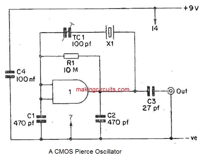
The inverter is biased into a linear amplifying mode by R1, and the crystal is linked amongst the input and the output of the circuit by means of TC1. This circuit, like the earlier design, functions at the series resonant frequency of the crystal.
There is absolutely no obvious favorable opinions loop amongst the output and input of the circuit, just the opposite in fact, considering that the input and output of the amplifier are in antiphase. At series resonance it might show up as though the crystal offers unfavorable suggestions to the amplifier.
This is simply not in fact the situation since C1 and C2 form a capactive centre tap on the crystal, with the centre tap being earthed. The crystal therefore performs as a type of transformer at series resonance, with its two connections in antiphase. There is as a result a 180 degree phase shift by means of both the amplifier and the crystal, and the opinions is optimistic.
TC1 is employed to cut the oscillation frequency of the circuit to the crystal's nominal frequency, and again, this feature can be ignored if preferred. TC1 is then avoided and the crystal is attached around R1.
C1 and C2 are demonstrated as possessing values of 470 pF each in the circuit diagram. Making use of these types of values the circuit should oscillate satisfactorily over a large amount of frequencies.
At frequencies above a few MHz it might be essential to reduce the value of these components fairly in order to acquire oscillation. On the other hand, at frequencies below a few hundred kHz a rather higher value may be needed for these components. Also, if highest output is needed it will likely be essential to discover the values of these capacitors by scientific means.
L-C Oscillator
A crystal oscillator is, obviously, designed to offer high firmness at a single frequency, and is useless if a tuneable wide range oscillator is needed.
These types of oscillator is practically invariably of the L-C variety for functioning frequencies of a few hundred kHz and above. CMOS I.C.s works extremely well as the basis of simple L-C oscillators, and an example of such a circuit is displayed below:-


This particular works at a frequency of around 465 kHz, and T1 is an ordinary broadcast receiver I.F. transformer. In normal use the tuned winding is the primary and the untuned one is the secondary, but here the windings are employed in the opposite roles.
This is merely a easy opinions circuit with the CMOS inverter getting used as a linear amplifier. The circuit can be tuned over a relatively narrow range of frequencies by using VC1.
As it stands here, the circuit is appropriate for use as an I.F. alignment generator or as a B.F.O. for a communications receiver. On the other hand, it will eventually work at frequencies above 10 MHz if a appropriate coil is employed (virtually any coil with a tuned winding plus a low impedance winding).
By increasing the value of VC1 to a couple hundred pF the circuit could also be designed to protect a wide tuning range. Remember that the circuit will never oscillate except if T1 is linked to the phasing demonstrated in the above A simple L-C oscillator diagram.
Hartley Oscillator
A CMOS inverter works extremely well in the popular Hartley type oscillator, and this has the advantage within the earlier design that just a single winding is required within the coil. Nevertheless, this need to be a centre tapped winding. The circuit diagram of a CMOS Hartley oscillator is shown in below diagram.

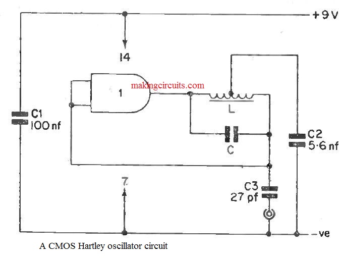
This is very identical in functioning to the pierce oscillator which was explained previously, the difference being that a centre tapped L-C circuit is employed instead of the capactively centre tapped crystal. The coil supplies a D.C. path amongst the input and output of the inverter, and so no bias resistor is required.
The circuit will certainly work over a frequency range of a few hundred kHz to greater than 10 MHz, and the values of L and C are chosen to fit the required operating frequency. C can be a variable capacitor if a variable frequency oscillator is essential.
Remember that the tapping does not have to be at exactly the centre of the winding, and that for example, the circuit will function completely well while using primary of an I.F. trans-former.
Phase-Shift Oscillator
An sound squarewave generator was included in the earlier chapter, and this is not the sole form of sound waveform generator which is often developed applying CMOS inverters. It is possible to produce a sinewave employing a phase shift oscillator, and such a circuit is displayed in below diagram.

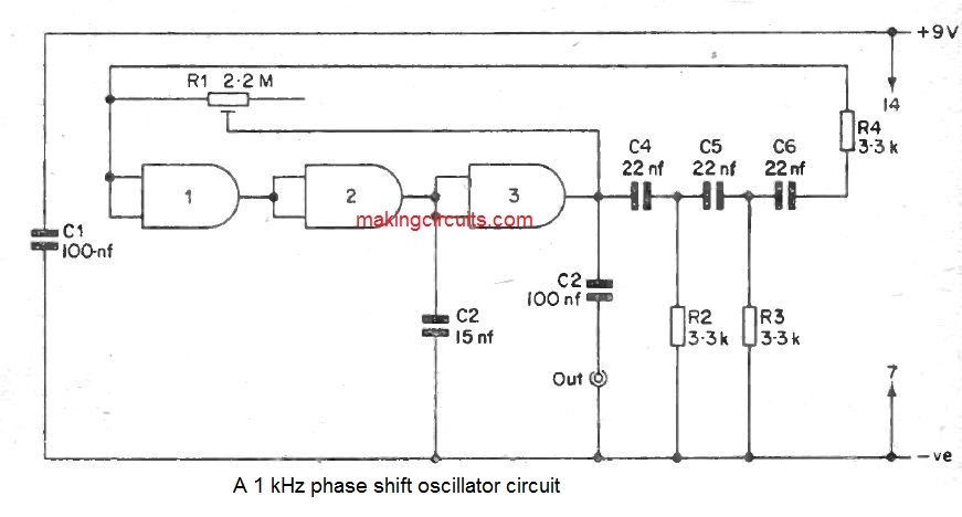
In this article three inverters are wired in cascade to create a high gain inverting amplifier. The actual gain of the circuit is regulated by the feedback network composed of R1 and R4. R1 has been conducted variable in order that the gain of the circuit can be arranged at exactly the needed amount.
The output of the amplifier is coupled to the input by way of the three 60 degree phase shift networks which includes C4 - R2, C5 - R3, C6 - R4. Therefore, at the functioning frequency of this network there is certainly optimistic feedback amongst the input and output of the circuit, and provided the gain of the amplifier is enough, the circuit will oscillate.
The gain ought to be no more than is totally essential as in any other case the output waveform will be altered. R1 is as a result modified for the lowest resistance that delivers reliable oscillation.
An functioning frequency of around 1 kHz is acquired using the particular values in the phase shift networks. This could be modified if needed, by replacing the values of C4 to C6. These should invariably be equal in value, and their value is inversely proportional to the functioning frequency of the circuit.
Hence employing 220 nF capacitors provides an functioning frequency of around 100 Hz, and 2.2 nF capacitors would deliver oscillation at around 10 kHz. The circuit will perform satisfactorily over a frequency range of less than 1 Hz to more than 20 kHz.
C2 is a stabilisation capacitor and C3 offers output D.C. blocking. The value of C3 ought to be increased if the unit is employed to feed a reasonably low impedance or if it is employed at a lower functioning frequency than
1 kHz.
Schmitt Trigger Oscillator
The circuit diagram of this strange circuit is demonstrated in below diagram. The three inverters are attached as a kind of Schmitt trigger, and this form of circuit is completely managed in the subsequent chapter. As a result only the features of the Schmitt trigger circuit will be viewed as, instead of exactly how this circuit in fact functions.

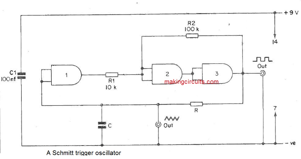
A Schmitt trigger has an output which includes only two stable states, and in this situation the output is normally high. By applying an appropriate input voltage the output could be designed to go to the low state.
With this particular circuit the input must be delivered to about half the supply rail potential ahead of the output will probably be triggered to the low state.
The output will go back to the high state again if the input voltage is reduced to a appropriate level, but the voltage at which the circuit activates back to the high state is less than the original threshold voltage. This characteristic is known as hysteresis.
It is extremely easy to be familiar with method by which this circuit functions. The output would go to the high state when the supply is in the beginning linked considering that the input will probably be low. Capacitor C then starts to charge up through resistor R.
When the voltage across C reaches the upper trigger threshold voltage, the output of the circuit goes low. C then starts to discharge by means of R and the output circuitry of inverter 3. When the voltage across C equals the lower threshold voltage of the Schmitt trigger, the output of the circuit will go high.
C then starts to charge through R yet again till the voltage across C reaches the upper threshold voltage of the circuit. The output then goes low again. C then starts to discharge, and the circuit constantly oscillates in this pattern provided that power is placed on it.
Two output waveforms are produced, a squarewave at the output of inverter 3, and a triangular waveform at the junction of R and C.
Variations in output load Impedance and supply voltage lead to relatively large variations in functioning frequency, and so in crucial applications it is essential to employ a buffer amplifier at the output and a stabilised power supply.
An unusual characteristic of this circuit is the wide frequency coverage which is often acquired in a single range if R is a variable resistor. For instance, employing a 2.2 Megolun potentiometer for R and a 470 nF capacitor for C, the circuit has an operating range of a few Hz to many tens of kHz. The circuit will oscillate at a frequency of around 1 kHz with C at
100 nF and R at 470 k.
A peak to peak output amplitude almost equal to the supply rail potential is acquired at the squarcwave output, but the triangular output amplitude is much lower, being something in the region of 100 mV peak to peak.
Furthermore, the triangular output is at a somewhat high impedance unless R has a low value. The circuit will oscillate with R possessing a value as low as a few tens of ohms, but for maximum reliability it should have a value of a few hundred ohms or more (the upper limit being many Megohms).
Simple Relaxation Oscillator using a Single BJT
The negative resistance area of a reverse-biased silicon transistor can be applied in a relaxation oscillator circuit. Its benefit is that an excess transistor is utilized instead of a UJT, which is generally more expensive, and it does deliver a minimum of components.

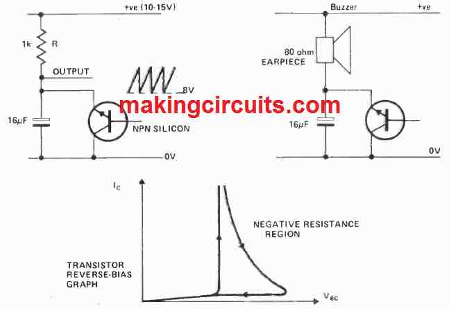
The frequency is controlled by the time constant RC, the power supply voltage and the area of the negative resistance region.
This zone also dictates the signal amplitude, so multiple transistors from a left-over batch can be examined for best results. The output formed is a sawtooth waveform with a mean DC level around 8 V. Once you replace the resistor with an 80 Ω earpiece, you will hear the resounding buzzer.