

The LF351 is an inexpensive very fast JFET input operational amplifier having an built-in clipped input offset voltage (BI-FET IITM technology). The unit uses a reduced supply current and still sustains a substantial gain bandwidth product and a extremely fast slew rate.
Additionally, well matched high voltage JFET input devices offer surprisingly low input bias and offset currents.
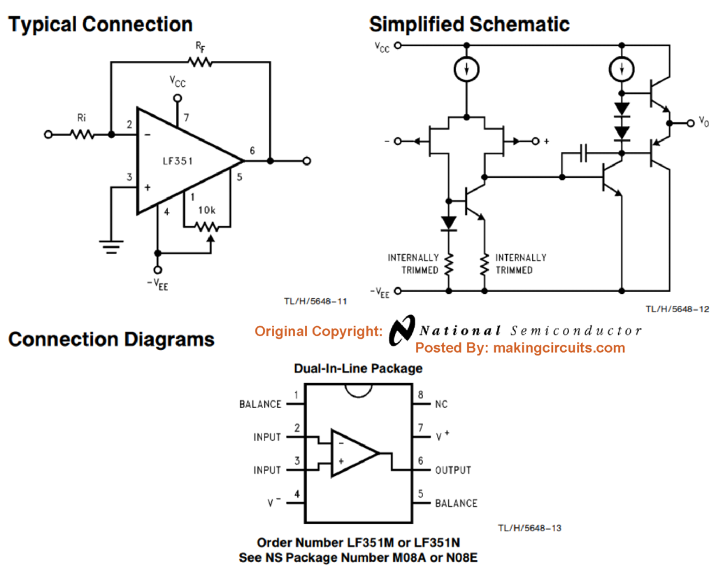
The LF351 is pin-to-pin compatible with the standard LM741 and employs exactly the same offset voltage realignment circuitry.
This characteristic permits users to promptly improve the efficiency of the standard existing LM741 models.
The LF351 can be employed in applications for example fast integrators and D/A converters, sample-and-hold circuits and several other circuits demanding minimal input offset voltage, high input impedance, low input bias current, high slew rate and wide bandwidth.
The IC features almost zero noise and offset voltage drift, however for applications in which all these necessities are essential, the LF356 strongly recommended.

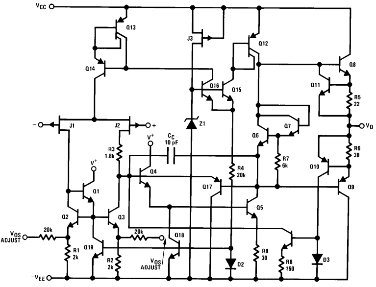
Detailed Internal Circuit Layout

Absolute Maximum Ratings
- Supply Voltage Never to be Crossed = +/-18V
- Power Dissipation without Heatsink applied = 670 mW
- Operating Temperature Range = 0° C to +70° C
- Tj(MAX) = 115° C
- Differential Input Voltage = +/-30V
- Supply Voltage Range on Input Pins = +/-15V
- Period for which Output can be held at Short Circuit = Continuous
- Storage Temperature Range = -65° C to +150° C
- IC Pin Temp. (Soldering, not to exceed 10 sec.) Metal Can 300° C DIP 260° C
How to Use IC LF351 (Precautions)
The LF351 is an op amp having an in-built clipped input offset voltage and JFET input devices (BI-FET IITM). These JFETs are equipped with massive reverse breakdown voltages from gate to source and drain getting rid of the usual clamping stages over the inputs.
As a result, substantial differential input voltages can be conveniently included without using significant boost in input current. The highest differential input voltage is not based on the supply voltages.
Having said that, none of the input voltages must be permitted to go beyond the negative supply otherwise this can lead to huge currents to move which often can cause a damaged IC.
Going above the negative common-mode threshold over either input may compel the output into a high logic condition, potentially leading to a output phase reversal.
Crossing the maximum negative common-mode restriction on either inputs might drive the op amp output into a high status. In neither situation does a latch happen because elevating the input back again within the range of
common-mode once again sets the input stage thereby reverts the amplifier within a normal working mode.
Crossing the positive common-mode threshold on a single input is not going to affect the phase pattern of the output; nevertheless, in case both inputs surpass the limit, the amplifier output will certainly be pushed into a high logic state.
The op amp may function using a common-mode input voltage same as the positive supply; having said that, the gain bandwidth and slew rate could possibly be dropped in this situation.
In the event the negative common-mode voltage shifts to within 3V of the negative supply, a rise in input offset voltage may possibly take place.
The biasing of the IC LF351 is implemented using a zener reference that enables normal circuit functioning on +/-4V power supplies. Supply voltages under this may lead to reduced gain bandwidth and slew rate.
The LF351 can handle a 2k Ohm load resistance to +/-10V through the entire temperature range of 0 degree Celsius to a70 dgrees C.
When the amplifier is compelled to operate larger load currents, in such cases, a rise in input offset voltage may possibly happen around the negative voltage swing and ultimately get to an active current control on each positive and negative shifts.
Safety measures must be exercised to guarantee that the power supply for the IC in no way gets reversed in polarity or that the device is never accidentally mounted oppositely within a socket, otherwise a large current spike over the ensuing forward diode inside the IC might lead to melting of the inner circuitry and cause a permanent damage to the opamp.
As with the majority of op amps, proper care must be undertaken with lead dress, part positioning and supply source decoupling in an effort to guarantee stability.
For instance, resistors from the output to an input must be put having the IC body near to the input to reduce ‘‘pick-up’’ and improve the frequency of the feedback pole by decreasing the capacitance from the input to ground. A feedback pole is established once the feedback close to any amplifier is resistive.
The input of the IC (normally the inverting input) having the parallel resistance and capacitance across the AC ground defines the frequency of the pole. In numerous circumstances the frequency of this pole is a lot higher than the anticipated 3 dB frequency of the closed loop gain and therefore you can find minimal impact on stability difference.
On the other hand, when the feedback pole is lower than roughly 6 times the anticipated 3 dB frequency a terminal capacitor must be inserted through the output to the input of the op amp.
Value of this capacitor needs to be such that the RC time constant of this capacitor and the parallel resistance it develops is higher than or corresponding to the actual feedback pole time constant.
Application Circuits
Now let's discuss a few application circuits using the IC LF351. Actually because this IC is an improved version of the IC 741 you can actually apply this IC for all the 20 DIY applications circuits, which I discussed in one of my earlier posts.
Below we see a few which were mentioned in the LF351 datasheet:
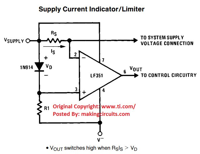
Current Limit Indicator Circuit
This circuit can be used for indicating the maximum current limit with high accuracy, when the current consumption by the connected load exceeds the set limit.
Thus this circuit using LF351 can be precisely implemented as over current cut off circuit also:

Variable Duty Cycle Pulse Generator Circuit
The op amp IC LF351 can be also effectively used as a variable duty cycle pulse generator within a range of extremely high and extremely low amplitudes.

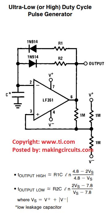
R1, R2 can be altered for changing the duty cycle ratio, while the 1M resistor can be tweaked for changing the amplitudes or the peak voltage of the pulses.
High Impedance Inverting Amplifier
Just like our own IC 741, the IC LF351 can be also rigged as an effective inverting amplifier but here it can be applied with an extremely high input impedance, higher than IC 741.
The detailed diagram is shown below:


In the above discussion we learned about the datasheet, pinout and application circuits of the IC LF351, which is an improved equivalent of the standard IC 741. If you have any specific questions regarding the topic, please do not hesitate to ask then through the comments below.