The FET amplifier features many pros than the bipolar transistor in amplifier circuits. For instance, the circuit designing techniques are exact or almost exact with the usual ones used for BJT circuits. Moreover, the high input impedance of the FET allows the standard flowing of RC-couple stages, without loss of gain between stages. An array of electronics like high-impedance devices, crystal microphones and pickups, piezoelectric transducers and capacitance-type transducers can be functioned into FET amplifiers.
Typical amplifiers circuits used in this discussion are provided with operating data which may vary so it is recommended to take note of the variations due to the spread in FET characteristics. In such cases, the transconductance spread can be quite high (over a range of 30:1). Furthermore, the input resistance (impedance) of each circuit can be amplified if needed by replacing a higher value of gate resistor. We recommend not crossing more than 22 mΩ.
FET Simple Small-Signal AF Preamplifier
A simplified, common source af FET amplifier containing a 2N3819 FET is depicted in Figure 2-1.
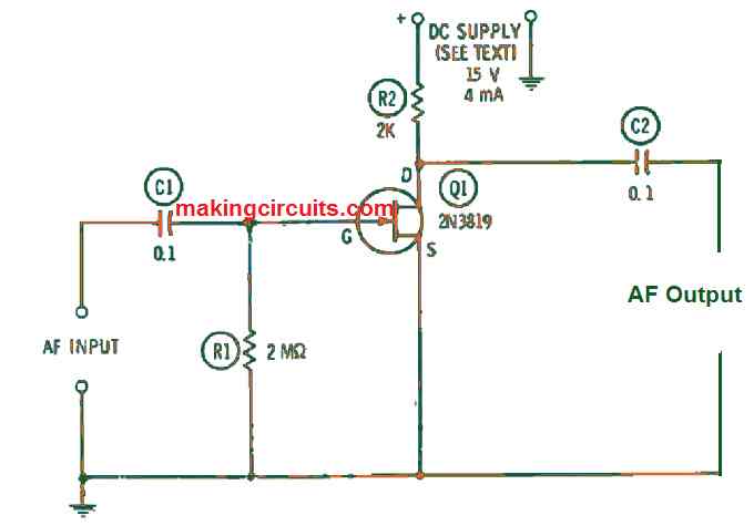
The source is grounded straight which allows this configuration suitable for af input levels below 0.6 V. When running at 6 V (2.5 mA) of the DC supply voltage level, the single stage provides a no-load voltage gain of 2.5 A at 9 V (3.1 mA) where the gain is 3.7. Additionally, at 15 V (4.0 mA), the gain is raised to 8. We will get a maximum signal input around before output-peak clipping reaches 0.58 Vrms. The frequency response is set to 1 kHz and falls falls in the range of 2 dB from 50 Hz to 50 kHz. The gain values are provided based on the 1 MΩ output load.
The 2N3819 is held in plastic and works well. All wiring is recommended to be kept as short and direct as possible. This is to alleviate stray pickup at the low signal levels at which this FET amplifier can run. The 2 MΩ gate resistor (R1) and 200 Ω drain resistor (R2) occupy 0.5 watt.
FET Single-stage, Low-gain AF Preamplifier
Through self-biasing the FET, higher gain than what was achieved by the preceding circuit and higher output voltage can be attained. A low-gain circuit similar like this which is based on a 2N4868 FET is displayed in Figure 2-2. You can see the source resistor R3 (bypassed by capacitor C3) delivers the needed gate bias. Moreover, this circuit is quite similar to the usual common-emitter bipolar transistor amplifier. Each resistor this circuit is rated 0.5 watt while the electrolytic capacitor C3 is rated 23 dcwv.
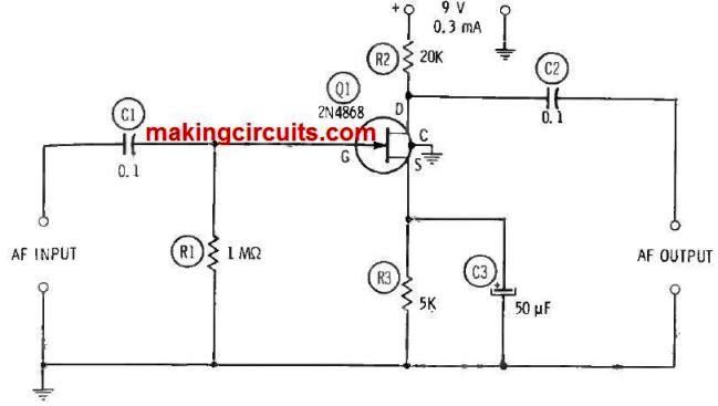
The open-circuit voltage gain is 20 when the DC supply is 9 V (0.3 mA). The maximum signal input before output-peak clipping is 50 mVrms while the corresponding output signal is 1 Vrms. Even in this case, it is crucial to keep the wirings short and direct to minimize stray pickup at the low signal levels at which this FET amplifier works. Just make sure one end of the 2N4868 is attached to the metal case of this FET and must be grounded for shielding purposes.
FET Single-stage, Medium-gain AF Preamplifier
Using the self-biased, common-source af preamplifier, which is based on a 2N4338 FET, as shown in Figure 2-3, we can get higher voltage gain than that afforded by the previous low-gain circuit. It can be noted that this circuit is identical to a common-emitter bipolar-transistor amplifier.
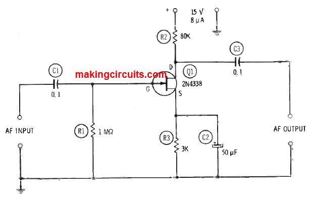
The open circuit voltage gain is 45 when supplied with 15 V (8 µA). The maximum signal achieved prior to output peak clipping is 78 mVrms. Consequently, a maximum signal output of 3.51 Vrms is obtained. The frequency response is 1 kHz and stays under 0.5 dB when ranging from 50 Hz to 20 kHz. When the frequency ranges from 50 Hz to 50 kHz, it stays under 4 dB. The 1 MΩ gate resistor (R1), 80 kΩ drain resistor (R2) and 3 kΩ source resistor (R3) are rated at 0.5 watt. The electrolytic capacitor C2 has a rating of 25 dcwv.
It is fundamental to ensure the wirings are short and straightforward to reduce stray pickup at the low signal levels at which this FET amplifier functions. We recommend exerting care in the area of 2N4338 because the gate electrode is internally attached to the metal case of this FET.
FET AF Source Follower
In Figure 2-4, you will see a circuit of a source follower employing a 2N4340 FET. It can be noted that using its un-bypassed source resistor (R2) across which the output signal voltage is established, this circuit is quite identical to its counterparts in terms of BJT-type emitter follower and bipolar-transistor emitter follower. Similar to the latter pair of circuits, the source follower is irreplaceable for transforming a high-impedance output to a low-impedance transmission line, corresponding a high-impedance transducer to a low-input-impedance transistor stage and so on.
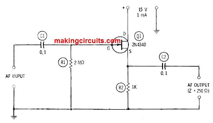
Using just DC supply of 15 V (1 mA), the voltage gain is 0.75 and the maximum signal before output-peak clipping is 0.7 Vrms. This contributes to a maximum signal output of 0.52 Vrms. Frequency response of 1 kHz is flat under 1 dB within the range of 50 Hz to 100 kHz. In this setup, the frequency response and gain are on a zero-load basis.
It was measured that the output impedance of the source follower is fairly lower than the 1000 Ω of source resistor R2. In this example, it is 250 Ω. This situation is identical to the conditions of the cathode follower and emitter follower. The components of the FET circuit show:
Ro = Rs / (1 + gmRs)
Ro = output impedance (resistance) in Ω
Rs = source resistance (R2 in Figure 2-4) in Ω
gm = forward transconductance of the FGET is mhos
Every resistor in this circuit is rate 0.5 watt and R1 can be increase as much as 22 MΩ if a higher input impedance is wanted. As always, the input circuit wiring must be managed short and straight forward as possible to alleviate stray pickup by this high-impedance circuit. Pay attention when looking for the 2N4340 and attaching it because the metal case of this FET is coupled to the gate electrode.
FET Two-stage, RC-coupled AF Amplifier
A big benefit of the high input impedance of the FET is its flexibility with old school RC-coupled multistage amplifiers. Limiting loss of gain between stages like what found in RC-coupled bipolar-transistor amplifier is not present in this circuit. From Figure 2-5, we can see a two-stage, RC-coupled amplifier containing two 2N4338 FETs. In this setup, cascaded, self-biased common-source stages are used.
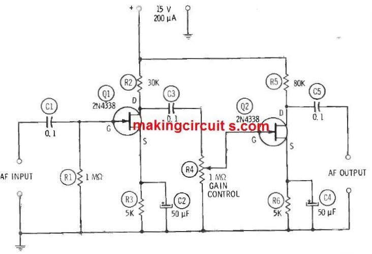
At 15 V, the total DC drain is 200 µA. When using this DC supple, the wholesome voltage gain of the FET amplifier is 1000 when potentiometer R4 is configured fully. The maximum signal input before output-peak clipping at this stage is 4 mVrms and this interacts to a maximum signal output of 4 Vrms. At 1 kHz frequency response, it will be don 4 dB at a range of 50 Hz and 50 kHz. Gain and frequency-response values are provided in relation to the 1 MΩ load across the output.
All resistors utilised in this experiment are rated 0.5 W. Electrolytic capacitors C2 and C4 are rated 25 dcwv. Like the previous circuits, it is crucial to keep the wiring short and direct to ensure minimization of stray pickup at low signal levels. We recommend using precaution when working around the area of 2N4338s because the gate electrode is internally attached to the metal case of this FET.
FET Two-stage, Transformer-coupled AF Amplifier
Because of the high input impedance of the FET, the transistor is very suitable for use as step-up coupling transformers between amplifier stages. It is also pretty standard in BJT amplifiers. The extra voltage gain because of the step-up turns ratio of the transformer can be achieved fairly easily. Instead, the low input impedance of the bipolar unit demands a step-down ratio in 1transformer-coupled bipolar-transistor amplifiers.
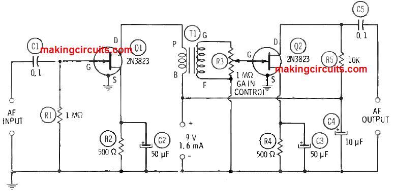
Figure 2.6 depicts the circuit of a two-stage FET amplifier holding transformer interstage coupling. At this point, transformer T1 delivers a 2:1 step-up, and it is quite a convenient BJT-type interstage transformer. You can see the typical primary (P, B) and secondary (G, F) labels. This FET amplifier is grounded on a pair of 2N3823 FETs (Q1, Q2). But the same plan may be deployed with different field-effect transistors. Some designers will prefer transformer coupling to surpass the low voltage amplification provided by low-transconductance FETs.
At 1 kHz, the voltage gain (with potentiometer R3 configured for full output, and the amplifier loaded with 1 MΩ) is 3000. This relates to a peak signal input of 1 mVrms for 3 Vrms output before output-peak clipping. For higher gain, a higher turns ration than the 2:1 value of the author’s transformer may be used. Frequency response of the FET amplifier is exclusively determined by the transformer. The sum of current drain of the circuit is 1.6 mA at 9 VDC.
You must make sure all leads are short and as direct as possible to reduce stray pickup and stray coupling. Additionally, the transformer container must be grounded. A fourth pigtail of the 2N3823 is attached to the metal shell of this FET and must be grounded for shielding purposes. All attached resistors as shown in Figure 2.6 are rated at 0.5 W while the electrolytic capacitors C2, C3, and C4 are valued at 25 dcwv.
FET High-impedance Input for Bipolar Transistor
An easy application of the FET is the establishment of high input impedance for a high-gain bipolar-transistor amplifier. At this moment, the FET works as an input-impedance transformer. Figure below displays a configuration like that. A 2N4340 FET source follower, just like the one described earlier, is linked before a high-gain stage occupying a 2N333 silicon transistor (Q2).

Just the 2N333 stage delivers a voltage gain of 200 when bias resistor R3 is regulated to an optimum value for the specific transistor used. Since the 2N4340 stage provides a voltage gain of 0.5, the total gain of the entire circuit is 100, when the output is ended with 1 MΩ.
The maximum signal input just before output-peak clipping is 20 mVrms and this refers to a signal output of 2 Vrms. The circuit operates around 1.04 mA at 15 VDC. All the resistors in Figure 2.7 are of 0.5 Watt whereas the electrolytic capacitor C4 is rated at 25 dcwv. You can make either R1 or R2 into a potentiometer for gain control, even if modifying R2 will deliver less noise.
FET High-input-impedance, High-gain Audio Preamplifier
The crossbreed audio preamplifier circuit depicted in Figure below is quite the same as the one discussed in the preceding section, but it suggests higher input impedance, lower output impedance and broader frequency response. Furthermore, it only needs a lower-voltage DC supply than the previous circuit.

Here, we utilise a FET (Q1) which is the heart of the high-impedance input stage. The FET is RC-coupled to a HEP S0015 silicon bipolar transistor (Q2) that delivers the lot of the gain of this preamplifier. The input impedance is about equal to the resistance of R5: 22 MΩ. The output impedance is around 25 kΩ.
The maximum input-signal voltage just before output-peak clipping is 45 mVrms and this generates an output signal of 2.25 Vrms; so, the total open-circuit voltage gain. ± 1 dB is the frequency response of the 1000-Hz value from 10 Hz to 100 kHz. Current drain is around 1 mA from the 9-V DC supply while all the resistors are rated 0.5 W.
FET Phase Amplifier
In Figure below, you can see the FET circuit of a classic two-way AF phase inverter founded on two 2N4338 FETs (Q1, Q2). The two outputs are 180° out of phase with the input signal; output 2 is in phase with the input signal.
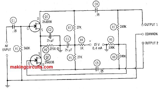
The circuit functions in the same way as the equivalent BJT-type circuit. This means, the signal is boosted and inverted by transistor Q1, and the output of Q1 (developed across resistors R7 and R6) is channeled to the OUTPUT 1 terminal. A share of this output signal is fed to the gate of the transistor Q2. Then, the signal is boosted and inverted by this transistor.
Q2’s output (which is developed across resistors R8 and R6) is supplied to the OUTPUT 2 terminal. Resistors R7 and R8 may work directly as the gate-to-ground resistors of a succeeding push-pull FET stage.
Similar to the equivalent BJT circuit, this phase inverter is self-balancing. This means the signal voltage established across resistor R6 by the output of transistor Q2 forces the signal voltage created across this resistor by Q1’s output (these two voltages are out of phase with each other).
This operation lessens the gate-to-ground signal voltage of a transistor Q2 and so keeps the signal at OUTPUT1 and OUTPUT 2 relatively the same. The inverter yields 0.4 mA at 15 V DC.
Capacitor C3 and resistor R4 create a decoupling filter that encourages stability. But these may be eliminated in some layouts if there is not problem from motorboating. All resistors are 0.5 watt and the electrolytic capacitors C2 and C3 are rated at 25 dcwv. In the 2N4338, the gate electrode is internally linked to the metal enclosure of this FET. So, you must exert caution when placing this transistor.
FET Paraphase Phase Inverter
A single-FET (“paraphase”) phase inverter, similar to the single-BJT circuit is depicted in Figure 2.10. This circuit that occupies a U183 FET, uses the 180° phase difference between the source output and drain output (same as the cathode output and plate output respectively). Additionally, it delivers the easiest configuration for transforming from single end to push-pull without using a transformer.

The signal at the OUTPUT 1 terminal is 180° out of phase with the input signal, that at OUTPUT 2 is in phase with the input. The equality of drain resistor R2 and source resistor R3, together with the huge amount of degeneration delivered by the unbypassed source resistor, holds these two outputs almost equally. (They must be normalized exactly through close adjustment of either R2 or R3, one with respect to the other). The circuit uses 0.25 A at 15 V DC.
The maximum signal input before output-peak clipping is 1 Vrms while the voltage gain in each half of the circuits is around 0.8. 1 kHz is the frequency response and it is flat within 3 dB from 50 Hz to 50 kHz. Gain and frequency response values are provided for 1 MΩ output load.
0.5 watt is the rating for all resistors and the electrolytic capacitor C2 is rated at 25 dcwv. A fourth terminal of the U183 is internally attached to the metal container of this FET and must be grounded as shielding precaution.
Is it possible to design this circuit with a 5V power supply?use other JFEF
If the FET is rated to work with 5V then it is possible…
thank you for posting this information it is very helpful
You are welcome!