In this post we detail the construction of a music triggered stroboscope light circuit,which can be used in parties or festive occasions for creating powerful strobe lights in response to music levels, through a xenon flash tube.
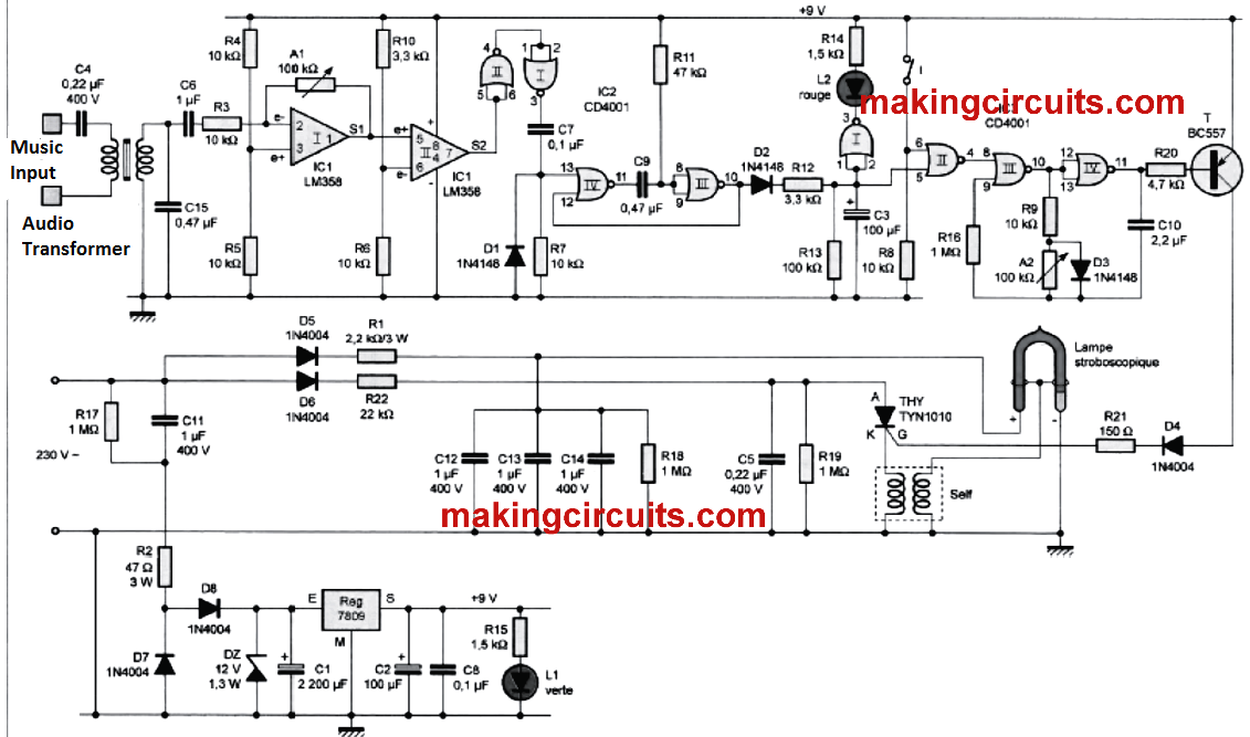
The power arrives from the 230 V mains through a capacitive coupling. In the course of an music pulses induce a periodic release of flashes at the amount ideal for illuminating a stroboscopic lamp.
The flashes continue throughout the duration of the music pulse.
We represent "positive" (by convention), the capacity C11 is packed through R2. Simultaneously, the capacitor C1 is charged via D8. The potential is methodically trimmed at 12 V, through the zener diode DZ (FIG. 1).
As soon as the subsequent "negative" (generally by convention) pulse takes place, the capacitance C11 could be discharged by R2 and the diode D7. This discharge of C11, furthermore accompanied by a load in the reverse direction, causes it as a result to manage the subsequent "positive" pulse and so on.
Alternatively, C1 is not able to discharge upstream given the blockage created by D8. Eventually, on the positive arm of C1, a rather undulated voltage of the order of 12 V is found.
This potential can now be placed on the Input of a regulator 7809 whose function would be to offer on its output a DC voltage and stabilized at 9 V. The capacitor C2 delivers supplemental filtering, while C8 will act as a decoupling capacitor.
The brightness of the green led L1, whose current is restricted by R15, alerts that the circuit is started up and the power supply is running correctly.
The resistor R17 discharges C11 once the circuit is turned off to be able to prevent the leads of this capacitor from remaining charged and are vulnerable to trigger debilitating jolts to the unwary novice coming in contact with them.
A music input leads to a variable and sinusoidal potential at a given frequency, the "minima" of which are at 0 V and the "maxima" at 10 V. This variable voltage is fed through C4 to one of the two secondary windings of audio transformer.
On the other winding of 6 V, is then accumulated a variable potential, because of the low capacity of C4 and characterized by peaks of 2 at 5 V.
Processing of the Music signal:
The Integrated circuit referenced IC1 consists of a couple of operational amplifiers. The "inverting" input of the amplifier (I) obtains the signals from the " 6 V winding of the transformer through C6 and R3.
The "non-inverting" input is afflicted by the supply half potential by the divider bridge shaped by
R4 and R5.
Therefore, it is this particular potential which can be found on the output S1 in the lack of signals.
However, when signals of a music comes from a source, the same signals are amplified on the output but amplified and aimed at the DC component of 4.5 V.
You are able to change the signals "Maxima" and "minima" by working on the slider of the adjustable A1. Within this type of amplifier, the gain is depicted by the relationship:
G = A1 / R3L
Amplifier (II) has its input (E1) afflicted by a fixed potential described through the values of R6 and R10. The value of the second option depends upon the relationship:
u = R6 / R6 + R10 * 9V
In our situation: u = 6.8 V
Therefore, so long as the potential from the output of the amplifier (I) On the input (e +) of the amplifier
(II) is no more than 6.8 V, the output features a "low" state at the waste voltage around, ie rather less than 2 V.
Positive pulses with an amplitude more than 6.8 V and input (e +), the output of the amplifier (II) provides
"high" states. The gates NOR (I) and (II) of IC2 perform a couple of effective inversions.
This leads to the same signal as that output from the output, Amplifier (II), however with "high" and "low" states correspondingly comparable to 9 V and to 0V.
Integration:
Every rising edge from the output of the NOR gate (I) of IC2 is evaluated by the differentiating stages formed by C7, R7 and D1.
Because of the quick charging of C7 through R7, there exists a sequence of positive positive pulses on the input (13) of the monostable flip-flop composed of the NOR (III) and (IV) gates, at intervals of 20 ms, Of IC2.
The second option then restores at its output a number of "high" states, calibrated each time based on the values of R11 and C9, consecutively to the relationship:
AT = 0.7 x R11 x C9
The viewer can confirm that The duration is approximately 15 ms.
The "high" states therefore produced result in the integrating method formed by D2, R12, R13 and C3. The capacitance C3 is charged by R12, throughout the "high" states supplied by the monostable flip-flop.
Alternatively, during the "low" states, it could only discharge in R13, of higher value.
Whenever the slider of the adjustable A2 is in the midsection placement, this period is about 0.2 sec. It will likely be observed that the slot is not really square in shape.
Certainly, the duration of the "low" states is a lot less than that of the "high" states. The main reason for this is the shunting of A2 by the diode D3 once the output of the oscillator is in the "low" state.
Generation of the Strobe flashes:
The strobe flashes are created by a strobe lamp of 30 to 40 joules. To be able to run effectively, such a lamp has to be subjected to a DC voltage of a minimum of 300 V.
This value is acquired by the load of capacitors C12, C13 and C14 attached in parallel, via R1.
The load develops every two alternations from the 230 V mains. Throughout non-active alternations, diode D5 offers the required blocking to stop discharge to the mains.
On the positive reinforcements of these capacities, a highest potential U is recognized in a way that: U = 230VxV2 is around 325V .
Another energy reserve, yet of much more moderate capacity, works based on the exact same theory. This is actually the load of C5 via D6 and R22.
Throughout the small "low" states provided by the oscillator, the transistor T, of PNR type, saturates. Consequently, it enables the circulation of a current, restricted to R21, in the "trigger -cathode" space of thyristor THY. The last mentioned starts instantly.
In this way a powerful, point-like current emanating through the positive arm of C5 through the "anode-cathode" junction of THY and one of the two windings of the triggering choke S. The winding under consideration is the one which Possesses few turns in accordance with the second.
Consequently, the control pulse goes through a very high voltage crescendo, that triggers the arc between the anode and the cathode of the strobe lamp, the power simply being supplied by the capacitors C12, C13 and C14. The lamp produces a brief, super bright light.
These capacities, along with C5, reload between 2 consecutive whizzes. The resistors R18 and R19 discharge the capacitors for the similar factors as those mentioned previously in the paragraph concerning the power supply.
PCB Design for the Music Strobe Light

PCB Component Layout

Leave a Reply