The earlier chapters are actually involved with circuits based upon easy inverters and gates, with all the projects being in line with the 4001 and 4011 I.C.s.
In this article we will learn how to make simple CMOS IC based circuits projects such as IC 4013, IC 4017, IC 4018, IC 4011, IC 4027 etc.
However these are just two devices from a huge collection of CMOS devices that happen to be currently accessible. It ought to be accepted that numerous of the I.C.s in this particular range are for extremely specialized applications, and are of minor use to the amateur enthusiast.
However, there are numerous devices which are often usefully hired by the
amateur, the frequency divider I.C.s being the most well known illustrations.
In this particular chapter, information on a few of the more dedicated CMOS IC will probably be provided, along with a few effective information on their use in easy CMOS projects.
Frequency Dividers
These are in general almost undoubtedly probably the most beneficial of the dedicated CMOS devices, and four types will probably be viewed as in this article.
These are the IC 4013 type D flip flop, the 4027 J-K master slave flip flop, the 4017 decade counter, and the 4018 presettable divide by 'N' counter.
The latter can be linked in order that it will certainly divide by any even number from two to ten (inclusive), and it will be talked about one at a time through the other three devices.
The easiest of the CMOS IC frequency dividers is the 4013, and this consists of two D type flip flops. To acquire this sort of circuit to divide by two it is simply essential to link the Q output to the data input, and earth the set anxi reset terminals. The input is then placed on the clock terminal and the output is extracted from the Q output.
Connection information for the 4013 are displayed in below diagram. If perhaps a single divide by two circuit is required, the clock input of the unused device ought to be attached to the negative supply rail. It is easy to achieve divide by four action by linking the output of one flip flop to the output of the other one.

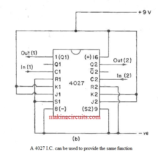
The 4027 I.C. consists of two J-K flip flops, and the circuit diagram mentioned below displays exactly how these are attached to offer a divide by two action. Once again it is easy to achieve divide by four action utilizing the two flip flops in series.
Connection details for the 4017 decade counter, or divide by ten circuit, is demonstrated in below diagram. This is extremely easy with the input being placed on the clock terminal and the output being extracted from the carry out terminal.

The reset and clock permit terminals should be earthed. An appealing characteristic of this device is that it has ten outputs in addition to the carry out one. These are generally marked '0' to '9' in above diagram.
These types of go high for one complete clock cycle in sequence. Therefore in the course of the first clock input cycle the '0' output will go higher, then the '1' output goes high for the next cycle, and so forth until the '9' output has gone , high for one cycle.
Then the entire sequence begins yet again right from the start. This element enables you to work the 4017 as a preset - table divide by N counter, but additional active circuit elements are needed, and in almost all situations it is simpler and less expensive to make use of the 4018 I.C. On the other hand, there are other applications through which this particular series of output pulses could be implemented.
Crystal Calibrators
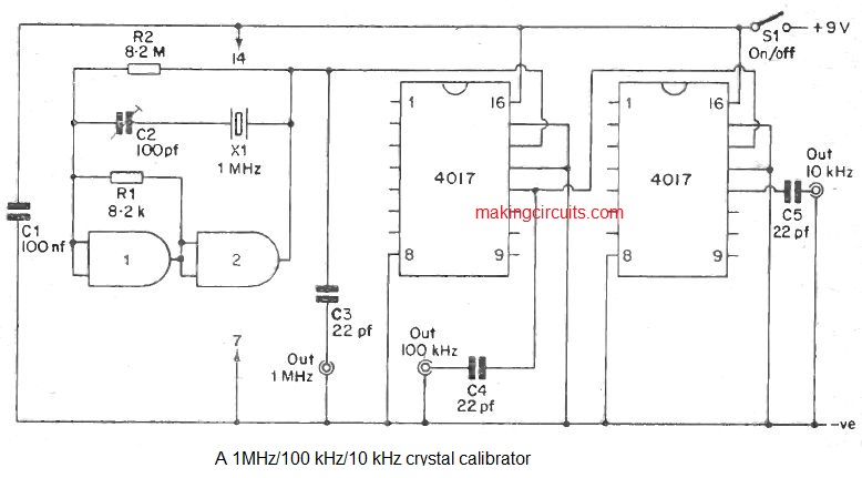
One of the main apparent use for a frequency divider is in a crystal calibration oscillator, and a easy circuit utilizing a 4017 in this part is revealed in below diagram:-

In this article quite a number of inverters are employed in a easy crystal oscillator of the type displayed previously in diagram a simple crystal oscillator circuit. This functions at a frequency of 1 MHz and has its output fed to the clock input of the 4017.
An output frequency of 100 kHz as a result shows up at the output of the 4017, and this circuit thus offers outputs at both 1 MHz and 100 kHz.
This could, obviously, be performed utilizing two different oscillators, one at each frequency, or by employing two switched crystals. This technique is more suitable though, since crystals are much more high-priced compared to 4017 I.C.
The outputs of this circuit have quick rise and fall times, and the outputs are as a result abundant in the specified harmonics. It offers marker frequencies at 1 MHz intervals from 1 MHz to over 30 MHz, and at 100 kHz time intervals from 100 kHz to over 30 MHz. The unit is thus well suited for calibrating general coverage M.W./S.W. receivers.
For the best possible accuracy to be received it is essential to trim the oscillator frequency to exactly 1 MHz.
Most likely the simplest way to achieve this is to link a lead to the 100 kHz output of the unit, and place this near to an operating receiver which is tuned to Radio 2 on the L.W. band. B.B.C. Radio 2 functions at exactly 200 kHz on the L.W. band, and the very first harmonic of the 100 kHz signal will respond with the Radio 2 signal to generate a beat note. This note will be very low in pitch, and C2 is adjusted to generate the lowest possible beat note.
With cautious tuning of the oscillator it ought to be feasible to acquire a beat note of lower than 1 Hz. For the majority of reasons such a high degree of accuracy is not really needed, and it is generally possible to acquire more than enough accuracy by departing out the trimmer capacitor (C2), and linking the crystal in parallel with R2.
Ibis worth noting that a majority of receivers have spurious reactions and inaccurate results can be acquired if the calibration signal is taken care of on one of these.
Because of this it is important to make use of merely a very loose coupling amongst the receiver and the calibrator, and it will most likely not be essential to make use of a direct coupling at all. Simply placing a lead attached to the suitable output of the calibrator near to the receiver's aerial socket ought to be sufficient.
Triple Output Version
In a diagram a simple 1 mhz/100 kHz crystal calibration oscillator circuit, is extremely good for calibrating general coverage receivers, but it results in a lot to be desired on the subject of the calibration of an amateur bands only set. As an illustration, the 80 Metre band extends from 3.5 to 3.8 MHz, and so the calibrator might simply offer calibration points at the band limits, plus two inside these limits.
Because of this it is extremely frequent for calibrators designed for use with amateur bands receivers to possess a really low output frequency furthermore to the standard ones.
This could effortlessly be accomplished using the circuit of diagram a simple 1 mhz/100 kHz crystal calibration oscillator by easily adding an extra decade counter at the 100 kHz output. This then gives outputs at 1 MHz, 100 kHz, and 10 kHz. The revised circuit is demonstrated in below mentioned diagram. This is set up and utilized in similar way as the original circuit.
Simple Calibration Oscillator
Despite the fact that L-C oscillators usually do not deliver this kind of fine accuracy and stability as crystal ones, it is however feasible to produce a flawlessly satisfactory calibration oscillator utilizing an L-C oscillator. The circuit diagram of this type of device is displayed in below:-

Inverter 1 can be used as an inductive feedback oscillator of the type used in the B.F.O./I.F. Alignment oscillator from diagram a simple L-C oscillator circuit. In this instance the tuned circuit is a Denco M.W. R.F. transformer, and the frequency of oscillation is tunable within the H.F. end of the M.W. band (around 1.7 to 0.8 MHz) by way of VC1. % n practice the oscillator is tuned to a frequency of 1 MHz.
Inverter 2 is employed as a sort of buffer amplifier, and the amplitude of the signal at its output is enough to effectively drive the clock input of the 4017 decade counter. A 100 kHz output signal is, needless to say, extracted from the output of the 4017. The unit as a result gives calibration signals at 1 MHz, 100 kHz, and their harmonics.
The circuit is placed up and employed in very similar method as the crystal calibrators, but it should be kept in mind the fact that crystal oscillators have just a very limited tuning range, although this circuit covers a fairly wide,range of frequencies.
VC1 will likely require a few modification prior to a beat note can be acquired. When a beat note has been acquired; VC1 is modified for zero beat in the same manner as for a crystal oscillator, however it is not likely that the unit are adjustable as exactly as a crystal oscillator.
The long term stability of this unit will never be as effective as that of a crystal controlled unit, and it is recommended to set the unit up against Radio 2 anytime it is utilized.
It is not a smart idea to solder direct to the pins of T1 as this has a polystyrene former which could melt with the heat of the soldering iron. The pins at the base of the coil will fit a B9A valveholder, and it is firmly advised that the coil is installed in one of these, and that the soldered connections are made to the holder.
The core of the coil is screwed all the way down once the coil is acquired, and it needs to be unscrewed a little bit so that about 10 mm of metal screwthread protrudes from the top of the coil.
The pin numbers demonstrated in above diagram an inexpensive 1MHz/100 kHz calibration oscillator demonstrate right phasing for the coil, and it is crucial that this is appropriate. There are actually three windings on the coil, but the one linked across pins 8 and 9 is avoided. The full explanation of the coil (which must be given when ordering it) is 'Yellow R.F. coil for transistor uscage, Range 2T'.
All the calibrator circuits demonstrated right here have used the 4017 I.C., but the oscillators could just as quickly be applied to feed a 4013 or 4027 device. In this instance the two halves of these I.C.s would be linked in series, and fundamental output frequencies of 1 MHz, 500 kHz, and 250 kHz would certainly be acquired.
It would not be possible to set these circuits up against Radio 2 on the L.W. band since there would be no output at 200 kHz, but the standard frequency transmission at 5 MHz could possibly be utilized rather.
The circuit in the above diagram A 1MHz/100 kHz/10 kHz crystal calibrator is not limited to utilize as a crystal oscillator, and circuits of this sort are located in many digital electronic circuits.
Frequency meters and electronic timers are common good examples. In such applications it will most likely be essential to include extra division phases, however this is very effortlessly achieved.
CMOS IC Risetime
One point that must definitely be borne in mind when employing CMOS frequency dividers is that for reliable procedure they desire an input signal possessing a fast risetime. The input waveform ought to have a risetime of less than 5 micro -seconds and ought to be more than 0.5 micro-seconds wide.
If a CMOS IC divider is to be used in effectively use from a slow input wave-form it must have some form of speed-up circuit added at the input.
The best way of obtaining this is to add a Schmitt trigger at the input, as displayed in below diagram. The way in which the Schmitt trigger functions won't be viewed as in this article as it was fully managed in the earlier chapter.

The best way it speeds up the input waveform is straightforward. As the input waveform increases it will have no impact on the output of the Schmitt trigger until it finally reaches the threshold voltage of the trigger. Then the output very rapidly swings positive and functions the divider. It is on the positive edge of the waveform that the divider is managed.
An Electronic Game
It was pointed out previously that the CMOS IC 4017 has ten outputs in addition to the normal carry out one. Five of these outputs are used in the circuit mentioned below which demonstrates the way the device may be used as the basis of an easy electronic game. It also displays the qualities of the 4017
I.C.
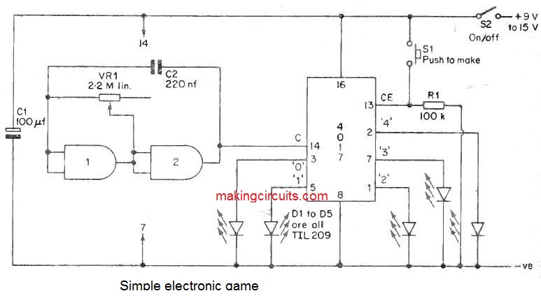
The two inverters are utilized in an astable multivibrator, and the working frequency of this could be varied from less than 1 Hz to over 100 Hz through VR1. The output of the multivibrator is employed to drive the clock input of the 4017.
The clock enable terminal of the 4017 is linked to earth by means of R1, and so when S2 is closed and power is applied to the circuit, the 4017 will begin to work. The first input cycle will result in pin 3 (the '0' output) to go high, and the first L.E.D. will illuminate.
At the beginning of the next clock input cycle pin 3 will resume the low state and pin 5 (the '1' output) will go high for one complete input cycle. Then pin 5 goes low and pin 1 goes high, and so on right up until all the
L.E.D.s have switched on in sequence.
There is then a pause during which none of the L.E.D.s can occur, and this is the period through which the unconnected outputs go high. When all five of these outputs have gone high the cycle starts off once more right from the start, using the five L.E.D.s turning on in sequence accompanied by a break.
In practice the L.E.D.s are installed in a row across the front panel of the unit, and the concept of the game is to stop the sequence when the middle L.E.D. (D3) is on. The sequence is stopped merely by pressing Si which is a push to make non -locking push button switch.
When this is controlled it takes the clock enable input high, and this blocks the clock signal and holds the 4017 in no matter what state it was in when at the instant Si was closed.
The circuit is reset ready for a new round by releasing Si. The sequence then proceeds from where it left off. The speed from which the circuit functions, and as a result the degree of problems, is regulated by the setting directed at VR1. The circuit can happen to be one that tests the reaction speed of the competitor, but it is actually more a test of coordination and anticipation.
It is feasible to make use of the circuit from a 9 volt supply, but the L.E.D. display will not be very bright and it is preferable to utilize a supply voltage of around 12 to 15 volts.
The 4018 Presettable Divider
Almost undoubtedly probably the most adaptable of the low-cost CMOS frequency divider I.C.s is the 4018 presettable divide by N counter. This is often utilized to divide by any even number from 2 to 10 inclusive. diagram mentioned below displays the essential connections to acquire a divide by ten action.

The fundamental method by which the device functions is pretty simple to implement. The clock signal is divided by 2 at the Q1 output, 4 at the Q2 output, 6 at the Q3 output, 8 at the Q4 output, and 10 at the Q5 out-put. In above diagram the 4018 os a decode counter circuit the Q5 output is coupled to the data input, and for that reason after ten input cycles the circuit is reset and the pulse count starts off again.
In order to acquire a divide by two action the Q1 output is attached to the data input rather than obtaining the Q5 input coupled to it. Connect the data input to Q2 for a divide by 4 action, to Q3 for a divide by six action, or to Q4 for a divide by 8 action.
In well-known while using other CMOS frequency dividers viewed as in this article, the 4018 will certainly work satisfactorily up to input frequencies of around 5 MHz when it is in combination with a 9 V supply line.
7 Segment Display Driver Circuit
Essentially the most beneficial and fascinating of the I.C.s in the CMOS IC range is the 4026 which is a decade counter and decoder. For the most part a separate decade counter and decoder I.C. are accustomed to produce a digital readout, but the 4026 performs both these functions and this significantly decreases the difficulty of digital systems through which it really is employed.
Another benefits of this I.C. over most others is that it does not need to drive the output display through either switching transistors or current restricting resistors. It could be accustomed to drive a low current seven segment display direct.
The author provides this device efficiently with a DL704E seven segment L.E.D. indicator, but it ought to perform equally efficiently along with any kind of related device.
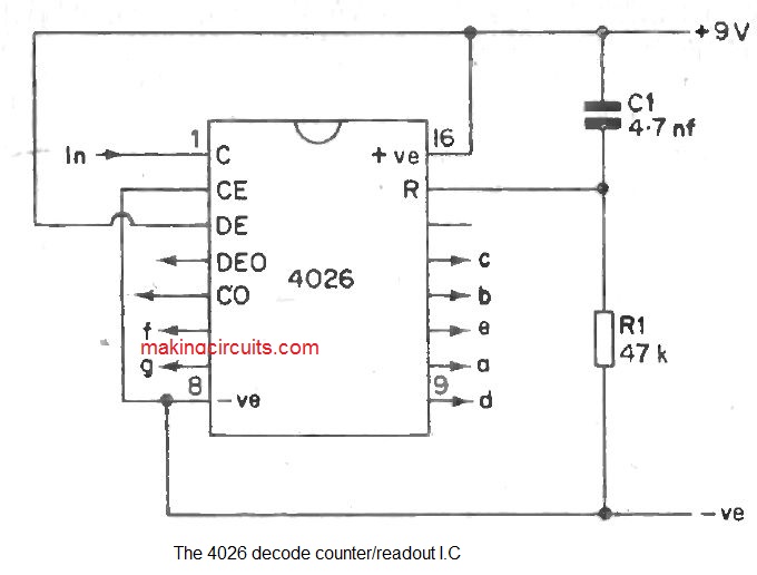
The circuit diagram demonstrated above exhibits what sort of 4026 could be linked to work as a simple pulse counter. The display displays the number of output pulses obtained at the clock input up to a maximum of nine, after which the display goes back to zero and commences counting up to nine once again.
In virtually all practical applications a maximum count of more than nine will probably be needed, and the circuit can be designed to count as high as one wishes merely by hooking up the carry out terminal of this circuit to the clock input of a second identical circuit.
The carry out input divides the clock input by ten, therefore, the first circuit counts the units (and drives the left hand display) while the second one counts the tens (and drives the right hand digit).
Undoubtedly, by adding further digits the circuit could be designed to count thousands, tens of thousands, and so forth. Remember that the 4026 can simply be applied to directly drive common cathode displays, and is not well suited for direct interface with common anode ones (for example the DL707E).
Besides the beneficial characteristics already stated, the 4026 has a few others. Pin 2 is a clock enable input, and the circuit functions generally when this is low, and fails to interact to input pulses when it is high.
In several applications the clock signal is fed to the counter circuit through an enabling gate. Once the 4026 is utilized in such applications a separate control gate is not really essential, and this input could be fed with the control signal instead.
When pin 3 is high the circuit performs in most cases, however when it is low the display is turned off. The I.C. is operative in all other respects. This is very beneficial mainly because it signifies that the display is effortlessly controlled, and need only be switched on when a reading is to be taken. Economic battery procedure is as a result possible where it might in any other case not be.
A display enable output is offered at pin 4, which could be employed to drive the decimal point of a display.
The reset input is generally attached to the negative supply by using a resistor, and the counter can be reset to zero by a brief positive pulse to this input.
In above diagram the 4026 decode counter/readout circuit I.C R1 ties the reset to earth and C1 offers a brief positive pulse at switch on which helps to ensure that the counter begins at zero. If a push button switch is linked in place of C1 it is possible to reset the circuit manually.
There are numerous applications for the purpose the 4026 is ultimately suited, but most of these are too difficult to come within the scope of this book. One simple novelty application is as an electronic random number indicator unit, and a simple circuit for one of these is found in below:-
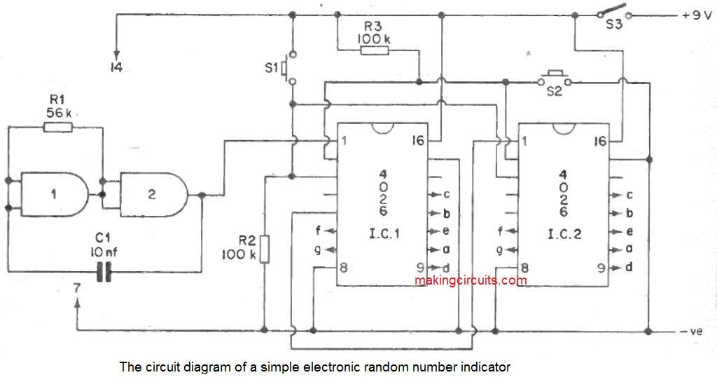
The two inverters function as a 1 kHz astable multivibrator and are utilized to feed the clock input of I.C.1. The carry out terminal of I.C.1 is in turn employed to feed the clock input of I.C.2. Both of these I.C.s plus the two readout devices thus form a two digit counter.
As the circuit stands, the display will be off and the clock signal will be muted. If S2 is pressed, the clock signal will operate the counter, and it will take the counter by way of a complete 00 to 99 count about ten times per second. When S2 is released, the counter will stop at whatever number it happened to be at at the instant S2 broke the clock enable circuit to earth.
What this number tends to be is fairly unpredictable, and in in this manner the circuit functions as a random number indicator. The unit could be designed to display the number by operating S1 which links the display enable terminals to the positive supply.
S3 is the normal ON/OFF switch.
Bilateral Switches
A bilateral switch is a type of enabling gate, except whereas most enabling gates are merely appropriate for employ with pulsed signals, a bilateral switch works extremely well in linear applications. For low signal levels the typical distortion level by way of a bilateral switch is merely around 0.4%.
There are actually two easily accessible CMOS bilateral switches, the 4016 and the 4066. These are generally either contained in a 14 pin DIL package and also have the pinning arrangement demonstrated in below diagram:-

The main difference amongst both of these devices is that the 4016 will work at frequencies up to around 10 MHz while the 4066 will continue to work around 40 MHz.
The on resistance of the switches is around 300 ohms and the off resistance is around 1 million Megohms. The switches are off when the control voltage is low and on when it is high.
Signal levels of about two volts peak to peak can be handled when these devices are operated from a single supply rail, however when operated from a dual balanced supply they can handle peak to peak signal voltages equal to the sum of the supply rail voltages
As will be apparent from above diagram the leadout diagram for the 4016 and 4066 I.C.s, the 4016 and 4066 devices each contain four bilateral switches, and this tends to make these devices very versatile.
It is worth noting that despite the fact that each switch has an input and output legend mentioned in above diagram the leadout diagram for the 4016 and 4066 I.C.s, this has only been carried out as it is far more convenient to consider during these phrases when thinking about practical functions for these devices, than simply using pin numbers for identification purposes.
These switches are, as their name states, bilateral, and in practice it would appear to be feasible to work with all of them in either case round.
These types of switches are merely single throw sorts, however it is quite possible to acquire a double throw action by making use of two switches with the outputs attached in parallel.
The control terminals of the switches ought to be fed from a circuit which usually helps to ensure that they may be forever in antiphase, with one switch in the on state and the other in the off situation.
This is often accomplished by feeding the switches through the Q and Q outputs of a flip flop circuit, for example the 4013 sort D flip flop. This type of circuit is demonstrated in below diagram.
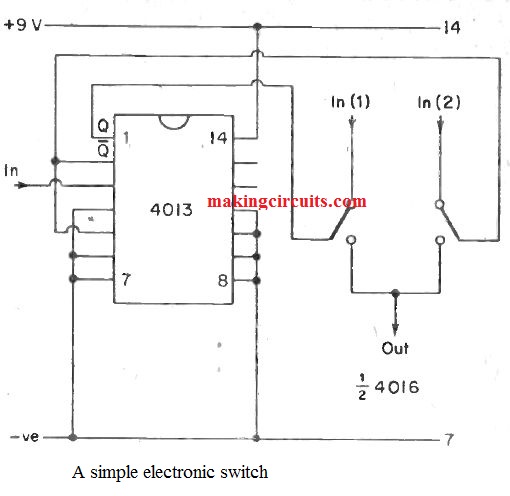
The 4013 is linked as a divide by two circuit with one of several two flip flops it includes getting unused. The two outputs of the 4013 are usually in the opposite logic state and these states change with each effective input pulse. If, as an example, the Q output is high and the Q one is, low when the power supply is in the beginning attached to the circuit, then input 1 will probably be allowed and input 2 will be blocked.
Applying a brief input pulse to the circuit will result in the flip flop to change state, and then input 1 will probably be blocked and input 2 will probably be enabled. The circuit hence offers a purely electronic S.P.D.T. switch.
A number of variations on this basic circuit are achievable. By paralleling the inputs rather than the outputs, the circuit will likely then channel the single input circuit to only one of two circuits linked at the output.
By simply omitting one of the bilateral switches a solely electronic S.P.S.T. switch is generated. By linking two further bilateral switches in the exact same settings as the original two, and feeding one control input from each output of the 4013, a D.P.D.T. action is acquired.
When thinking about making use of these types of switches often keep in mind the restrictions on both the signal amplitude and impedance.
For instance, the D.P.D.T. version of this switch could hardly be applied as the send/receive switch of an intercom, as even though it might probably be designed to handle the signal amplitudes by utilization of a dual balanced supply, the 300 ohm series resistance of each switch would certainly limit the output to the speakers to an unsatisfying level.
The 4016 device is particular in the circuits explained in this article since there are hardly any applications in which the additional efficiency of the 4066 is needed, and the 4016 costs less and much more easily and widely available.
CMOS Touch Switch
In simple applications a touch activated version of the circuit in above diagram a simple electronic switch is most likely associated with much more use. This type of circuit shows up below mentioned diagram.
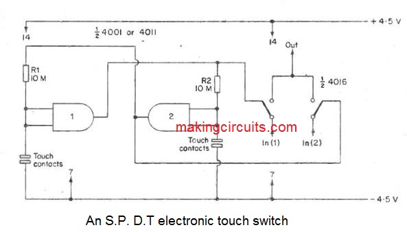
In this article two inverters are employed as a bistable multivibrator with high value cross coupling resistors. Tends to make the circuit adequately delicate to be operated by touch contacts.
We are going to believe in the interests of this circuit description that the circuit occupies the state of possessing inverter 1 output low and inverter 2 output high when the supply is in the beginning linked (even though it might actually started the opposite state).
To be able to trigger the circuit into the opposite state, and so reverse the states of the bilateral switches, it is simply essential to touch the left hand set of touch contacts.
This takes the input of inverter 1 low since it will probably be linked to earth with the skin resistance of the operator. This particular sends the output of inverter 1 high which inturn takes the input of inverter 2 high due to the coupling by using R2.
Inverter 2 output as a result goes low, and inverter 1 input will as a result remain in the low state even though the operator's finger is taken out of the touch contacts, since it will be held low by being coupled to the low output of inverter 2 by using R1.
The circuit can be reset to the original state by touching the right hand set of touch contacts. Equivalent circuit action after that occurs, however the roles of the inverters are reversed this time around.
You are able to trigger the circuit from one state to another consistently by functioning each set of contacts in turn. There are, obviously, no moving parts no matter what to wear out, As was the case with the above circuit diagram a simple electronic switch , a number of variations on this basic circuit are possible.
CMOS Audio Squelch
Squelch circuits are usually utilized in F.M. tuners and receivers, and in V.H.F. communications devices. With this particular form of devices there exists a high level of background noise in the lack of a signal, and the reason for the squelch circuit is to mute the receiver unless a signal is present.
This particular gets rid of the very loud and therefore irritating background hiss that happens when tuning an F.M. set amongst stations, or when no signal is found at the input of a V.H.F. communications set.
When it comes to this kind of devices the squelch circuit is generally triggered by the carrier wave signal of the received transmission, instead of by the audio signal.
In this article you will find, audio applications in which a squelch circuit can be handy. One of these will be in the matter of, a public address system which can be employed in a noisy environment, with a relatively higher background noise level being transmitted within the devices.
In this instance the squelch circuit will be modified so that it may not be triggered by the normal background noise level (of human instead of an electrical origin), but in order that it might simply enable the equipment in the existence of a correct microphone signal.
There needs to be a number of other applications for this kind of equipment in addition to this one, and this is an application that on which the 4016 is preferably appropriate.
The circuit diagram of an audio squelch unit making use of the bilateral switches in the CMOS 4016 I.C. is demonstrated in below diagram:-

Procedure of this CMOS IC circuit is fairly uncomplicated. Some of the input signal is fed to the input of the bilateral switch and the remainder is fed to a high gain common emitter amplifier by using a gain control (VR1) and a D.C. blocking capacitor (C2). Tr1 is the basis of the amplifier and this has collector load resistor R1 and base bias resistor R2.
The output of this amplifier is fed to a rectifier and smoothing network utilizing C3, D1, D2, C4 and R3. The output of this network is fed to the control input of the bilateral switch.
VR1 is adjusted in order that the control voltage fed to the bilateral switch is inadequate to allow the switch with merely a background signal being fed to the input, but it is modified to ensure that this voltage is only just lacking the trigger voltage of the switch.
As a result, when a proper input signal exists, the trigger voltage will be exceeded and the switch will probably be allowed. The unit hence offers the needed squelch action.
It is probably not completely right to call the voltage at which the bilateral switch changes state a trigger voltage, since this refers to that the switch can simply be fully on or fully off.
This is simply not the situation, and there is a range of control voltages over which it will likely be in an advanced state. Thankfully on the other hand, this range of voltages is very limited, and the 4016 has a relatively well-defined changeover voltage.
This particular circuit as a result functions satisfactorily in practice with no need to incorporate any triggering.
The circuit has a fast attack and slow decay (hysteresis) which is essential to make certain that the unit does not cut off through the brief pauses which take place in the course of normal speech.
The decay time could be altered to suit individual specifications by modifying the value of C4. The decay time is proportional to the value of this component, and it is something lower than one second with the value demonstrated above diagram an audio squelch unit circuit.
Satisfactory procedure of the device is achievable with a nominal signal input level of lower than 100 mV R.M.S. to a a bit more than 1 V R.M.S. (sinewave input). The input impedance is around 10 k. Tr2 and connected parts form an emitter follower output stage which supply the unit with a low output impedance.
C3 must be a high quality component if it is an electrolytic kind, and it would possibly be recommended to make use of a tantalum bead or plastic foil component in this article. Some electrolytic types have fairly high leakage currents which may result in the decay time of the circuit being greatly prolonged.
Automatic Cutout
This circuit is designed for use with disco and home movie equipment in which the facility to automatically cut out a secondary channel (playing background music for example) by making use of a signal to the main input (like a commentary) is needed. The circuit diagram of this unit is demonstrated in below diagram:-

The controlled input is fed to a gain control, and then to a bilateral switch. From here it is fed to the output by way of mixing resistor, R1.
A few of the main input is fed to achieve control VR3, and then to mixing resistor R5. VR1 and VR3 enable the two input signals to be well balanced to the needed levels at the output. A few of the input signal at the main input is fed to a high gain common emitter amplifier by means of gain control (VR2) and D.C. blocking capacitor (C4).
The output using this amplifier is fed to a rectification and smoothing network utilizing C2, D2, D1, C1 , and R2. The output of this network is fed to the control input of the bilateral switch.
When no input signal is fed to the main input, the control input of the bilateral switch will be at earth potential, but as this is a positive earth circuit the control input is in fact high, and so the switch is enabled.
The controlled signal is as a result fed to the output.
If an input signal of adequate level is placed on the main input, the negative D.C. bias developed around R2 and C1 will be practically equal to the supply potential, therefore, the control input of the bilateral switch will probably be taken low, and the controlled input will be blocked. Thus the main input may be used to cut out the controlled orfe.
VR2 is given any setting which usually permits the main input to regulate the secondary one without having unfounded disruptions of the controlled input occurring. A minimum input amplitude of around 100 mV is essential at the main input in order to cut off the secondary input.
As was the case with the earlier circuit, the diode feed capacitor
(C2) should be high quality electrolytic type, or a plastic foil component.
Furthermore in common with the earlier circuit, this method has hysteresis, with the decay time of the circuit being variable through C1.
Hi,
Thanks for the Audio Squelch Circuit and the excellent lucid and comprehensive explanation which accompanied it. So often it is the explanation of a circuit which is lacking!
Pat
Thanks, glad you found it useful.