Looking for simple sinewave inverter circuits, which can be customized as per your specific needs? The following ideas may help you to achieve your objectives
A sinewave inverter is a device that converts DC power (batteries, accumulators) into alternating current (typically 220 volts 50 Hz sine or corrected). Our common emergency power supply, the general is the DC battery into 220V AC. In simple terms, the inverter is a device that converts direct current into alternating current.
Whether in the remote village, or the field needs or power outage, the inverter is a very good choice. The more common is the engine room will use the UPS power supply, in the event of a sudden power outage, the UPS DC inverter can be converted into AC for the computer to use, so as to prevent a sudden power outage caused by data loss.
This article will introduce two relatively simple sinewave inverter circuit diagrams. And it shows that interested friends can study, do it yourself to do an inverter is indeed a very sense of accomplishment. One is a more common inverter circuit diagram.
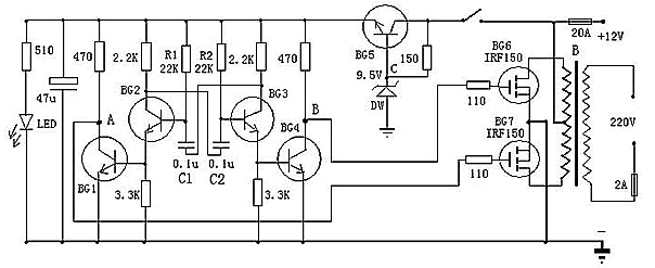
The above is a relatively easy to produce the inverter circuit diagram, you can 12V DC power supply voltage inverter 220V mains voltage, the circuit from BG2 and BG3 composed of multi-harmonic oscillator to promote, and then BG1 and BG2 drive to control the BG6 And BG7 work. The oscillation circuit by the BG5 and DW group of power supply, so that the output frequency can be more stable. In the production, the transformer can be used commonly used dual 12V output mains transformer. According to the need to select the appropriate 12V battery capacity.
The following is a high efficiency sine wave inverter electrical diagram, the circuit with 12V battery-powered. First with a double voltage module voltage for the op amp power supply. The ICL7660 or MAX1044 can be selected. Op Amp 1 generates a 50 Hz sine wave as the reference signal. Op amp 2 as an inverter. Op amp 3 and op amp 4 as a hysteresis comparator. In fact, op amp 3 and switch 1 constitute a proportional switching power supply. Op amp 4 and switch 2 are the same. Its switching frequency is unstable. In the op amp 1 output signal is positive phase, op amp 3 and switch work. At this time op amp 2 output is negative phase. At this time op amp 4 positive input potential (constant 0) than the negative input terminal potential is high, so the op amp 4 output constant 1, switch off. In the op amp 1 output is negative phase, the opposite. This enables the two switches to work alternately.

When the reference signal than the detection signal, that is, op amp 3 or 4 of the negative input signal than the positive input signal higher than a small value, the comparator output is 0, switch tube is open, followed by the detection signal quickly increased, when the detection signal Compared with the reference signal is higher than a small value, the comparator output 1, switch off. It should be noted that the comparator has a positive feedback process when the circuit is flipped, which is the characteristic of the hysteresis comparator. For example, under the premise that the reference signal is lower than the detection signal, the reference signal is immediately higher than the detection signal at a certain moment as their differences are close to each other. This "certain value" affects the switching frequency. It is the lower the frequency.
C3, C4 role is to allow the frequency of the switch freewheeling current through, and the lower frequency of the 50Hz signal to produce a larger impedance. C5 is calculated by the formula: 50 =. L is generally 70H, the best time to make a test. So that C is about 0.15μ. R4 and R3 ratio should be strictly equal to 0.5, large waveform distortion significantly, small can not start, but would rather large, not small. The maximum current of the switch tube is: I == 25A.
The existing inverter, there are two kinds of square wave output and sine wave output. Square wave output of the inverter efficiency is high, for the use of sine wave power design of the electrical appliances, in addition to a small number of electrical appliances do not apply to most of the electrical appliances are applicable, sine wave output inverter does not have this shortcomings, but there Inefficient shortcomings, how to choose this need to be based on their own needs.
Sinewave Inverter Circuit using Bubba Oscillator
This next article shows ways to Build a Sine Wave Inverter Circuit using Bubba Oscillator
The much anticipated sine wave inverter by means of bubba oscillator might be recognized with the aid of the following points:
The stage consisting two 555 ICs are set up as PWM generators where IC1 forms a square pulse generator for the PWMs while IC2 forms the monostable PWM generator with regards to the modulation input applied at its pin5.
The sine wave modulation input at pin5 of IC2 is ahieved by making use of a bubba oscillator produced by utilizing four opamps from the IC LM324.
The produced sine wave pulses are set at accurate 50 Hz and given to pin5 of IC2 via a BJT common collector for even more processing.
The 50 Hz for the bubba oscillator is placed by choosing R exactly with the aid of the following formula:

Before learning How to Build a Sine Wave Inverter Circuit using Bubba Oscillator it's important to learn something about bubba oscillator
The Bubba oscillator is a unique form of phase shift oscillator. The idea employs 4 levels to deliver an incredibly steady output frequency.
The accessibility of quad op amp integrated circuits helps make execution specifically effortless. Every one of the 4 op amps includes a matching RC network exterior to the chip.
All these networks adds a period shift of 45 , to get a overall phase shift of 180 , that is certainly required to position the answer in the transfer functionality in oscillation. Acquiring 4 levels likewise helps to keep the rate of change of period with regard to time adequately reduced for better efficiency and balance.
As soon as the signal advances via each op amp, the feedback expression (B in the diagram in figure 1) will probably be 1/4
Considering that we'd like genuine part of the answer, A*B, of the transfer equation to become comparable to one, the gain of the Bubba oscillator should be 4. The Bubba oscillator will take advantage of op amps in a buffering topology in order to avoid loading among every single op amp.
The stability of the frequency becomes a great deal better at each subsequent level.
You possibly can tweak the frequency at prior stages in the circuit, nevertheless efficiency might be affected. Such as, the total harmonic distortion following the second stage could be a whole lot worse compared to after the 4th stage.
In various other programs, in case a more serious total harmonic distortion is bearable in the layout, tapping within a prior position can help you save space and cost, given that much less components will be essential.
Simple 500VA Pure Sine Wave Inverter Circuit
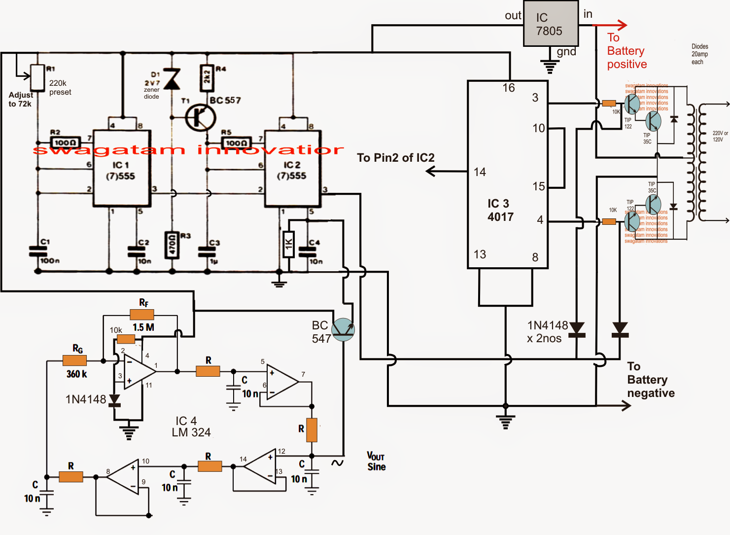
Let's try to work out the proposed simple 500VA Pure Sine Wave inverter circuit layout elaborately with the following facts:IC2 and IC3 are in particular designed in the form of the PWM generator step.
IC2 shapes the high frequency generator essential for the switching the PWM waveform which happens to be treated by IC3.
For working the IC2 oscillations, IC3 is required to be supplied through a sine wave comparative instruction at the pin#5, or the control input of the right IC 555.
Considering that producing sine waveform is somewhat challenging compared with a triangular waves, the triangle was favored because it looked much easier to render nevertheless works pretty much a sine wave counterpart.
IC1 is connected up as the triangle wave generator, whose result is ultimately applied to pin#5 of IC3 for the building the expected RMS sine similar to at its pin#3.
In spite of this the above refined PWM signals must be modulated over a push-pull version of design to ensure the waveforms have the ability to charge the transformer with alternately operating current.
This could be required for accomplishing an secondary mains made up of equally positive as well as the negative half cycles.
The IC 4017 is brought in mainly for enacting this function.
The IC produces a in sequence jetting output from its pin#2 to pin#4, to pin #7, to pin#3 and returning to pin#2, in accordance with just about every ascending pulse side at pin #14. This pulse is created from the output of IC2, which is basically determined to 200 Hz precisely to ensure that the outputs of IC4017 ends up with a 50 Hz throughout the sequencing from the above mentioned pin outs.
Pin#4 and pin#3 are specifically ignored, for making a killed zone around the gates sets off of the corresponding transistors/mosfets plugged into the pertinent outputs of IC4017.
This dead time takes care that the fets by no means switch ON collectively possibly even for a nano second at changeover periods, thereby safeguards the well-being of the gadgets.
The running positive outputs at pin#2 and 7 activate the corresponding fets which then compel the transformer to saturate with the AC power supply brought on in the specific winding.
This leads to the procreation of approximately 330+ V AC at the secondary of the transformer.
Nevertheless this voltage could well be a square wave with excessive RMS if this might not be treated with the PWM from IC3.
Transistor T1 together with its collector diode is applied with the PWM pulses in ways that T1 at this point runs and grounds the base volatge voltages of the outputs fets in keeping with the PWM information.
This contributes to an output that may be a definite reproduction of the the applied PWM fully optimized feed..... building absolutely etched pure sine wave AC counterpart.
The explained 500VA Pure Sine Wave inverter circuit possesses other highlights for instance a manual output voltage modification circuit.
The a couple of BC108 transistors are stationed for regulating the gate commute voltage degrees of the mosfets, the base current these particular transistors originate from a tiny sensing winding on the transformer which supplies the demanded output voltage measure data to the transistors.
In the event that the output voltage should go beyond the anticipated normal intensity, the base volatge of the above transistors could possibly be realigned and cut down by adjusting the 5K preset, consequently bringing down the conduction of the mosfets, eventually straightening out the output AC to the preferred boundaries.
The BD135 transistor together with its base zener presents a stabilized voltage to the involved electronics for perpetuating constant PWM output from the pertinent ICs.
Using IRF1404 being the mosfets, the inverter have the ability to yield approximately 300 to 5000 watts of pure sine wave output.
Submitted By Ravi Singh

A few drawbacks and flaws were found while carrying out a close inspection of the above circuit details. The improvized circuit (hopefully) is presented below.

The above 500VA Pure Sine Wave inverter circuit could be even more enhanced using an automatic output correction feature as indicated below. It is executed by introducing the LED/LDR opto-coupler stage.

سلام pcbاینورتر سینوسی بوبا رو از کجا تهیه کنم
Sir, what value should I put for R1, R2, C1 to get 50Hz?
A jeyaamirtharaj, please put a preset (variable resistor) in place of R1, with a series 10k resistor, and adjust this preset to get 50Hz output frequency. You will need an oscilloscope to check the waveforms…
Which wave did first circuit produce
How many watts does the first circuit has.., and value of the BG 1-5
100 watts.
BG1 to BG5 = BC547
Could some body tell me which of all this schematics are REALLY PURE SINE OUTPOUT? Regards
the bubba oscillator will produce almost pure sine wave
Looking SG3525 configarastions
What is the value of BG1, BG2, BG3, BG4 and BG5 on the first Circuit Diagram.
What is BG1, BG2, BG3, BG4 and BG5.
you can use BC547 for them
LDR LED added is not clear connection
Many thanks for your kind answer. I’ll build this inverter to power various ex-avio electronic devices. Best regards
Thanks for your feedback, appreciate it a lot!
Thanks for the interesting inverter circuits.
I am interested in the inverter with the stabilization of the output voltage, but with a frequency of 400 cycles and power of 100 watts. I would like to know: ic 2 and ‘cd4017? The mosfets are irf540 or 840 ?The supply voltage is 12vdc? and finally the transformer has a primary for 12 volts with central tap?
Thank you
Julian
Thanks, the bottom IC is 4017, rest all ICs are IC 555 or LMC555.
Here’s the correct diagram with load control
https://makingcircuits.com/wp-content/uploads/2019/06/IC-555-sine-wave-inverter-circuit.png
Hello Sir.
I don’t have a frequency meter to be able to get the respective 200hz, 500hz and RMS values at the respective preset variable resistors.
Can I get a fixed value for each of them for a 50hz setup?
The MOSFETs are IRF540, battrey is 12V, transformer is 8-0-8 or 9-0-9
Thanks for the inverter circuits. Since it is a bit technical stuff, so most people don’t know much about it.
No problem, you can feel free to ask your queries here, I will be most happy to help….