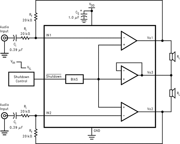
The circuit diagram of the LM4910 stereo headphone amplifier is witnessed above. C1 and C2 are actually the input DC decoupling capacitors for the left together with right input channels. R1 along with R2 tend to be the individual input resistors. R3 is the feed back resistor for left channel whereas R4 is the feed back resistor for the right channel. C3 is the supply of power filter capacitor. The feed-back resistors additionally implements the closed-loop gain together with the involved input resistors.
Notes.
The IC can be purchased basically in SMD packages and proper care need to be applied while soldering.
The circuit could very well be operated from approximately between 2.2V to 5V DC.
The headphone load could possibly be a 32 ohm headphone.
Total optimum supply voltage is 6V and approximately above may well ruin the IC.
A logic low voltage at the shutdown pins shut downs the IC and a logic high voltage at the comparable pin activates the IC.
the LM4910 has about three operational amplifiers in house. A couple of the amplifier's include on the surface configurable gain although the other amplifier is usually internally predetermined at the bias point behaving as a unity-gain buffer.
The closed-loop gain of the two configurable amplifiers is defined by opting the ratio of Rf to Ri.
As a result, the gain for every channel of the IC is
AV = - (Rf/Ri) ------- Eq#1
By just operating the loads by means of outputs VO1 and VO2 with VO3 working like a buffered bias voltage the LM4910 is not going to call for output coupling capacitors.
The standard single-ended amplifier setup in which one particular aspect of the load is linked with ground demands huge, pricey output coupling capacitors while Building a Stereo headphone amplifier
The construction like the one included in the LM4910 features a significant edge over single supply, single-ended amplifiers.
Because outputs VO1, VO2, and VO3 are generally biased at VREF = 1.58V, simply no net DC voltage is available throughout each load.
That gets rid of the importance of output coupling capacitors that happen to be recommended inside a single-supply, single-ended amplifier setup.
With no output coupling capacitors inside a regular single-supply, single-ended amplifier, the bias voltage is defined along the load which results in either elevated interior IC power waste and probable loudspeaker problems.
POWER DISSIPATION
Energy waste can be a serious worry when making an effective amplifier. An immediate outcome of the higher power transferred to the load by a bridge amplifier can be an escalation in inside energy turbulence.
The highest power waste for any presented application could be produced by the power dissipation chart or from the earlier equation.
Another Headphone Amplifier Circuit using Op amps
A simple yet extremely hi-fidelity type Stereo Hi-Fi Headphone Amplifier Circuit can be studied in the following article which will give you an of the world experience once you build it and start using it

The four diodes in rectifier bridge B1 are bypassed with rattle suppression capacitors to ensure minimum noise on the supply rails to the opamps.
This makes it possible to feed the 15V regulator from the raw voltage across Ca (+) and C10 (-) of the existing l8.5 V supply while the inputs of the volume control of the head- phone amplifier are driven direct from the outputs of IC4 l l (R) and IC4’ (L).
At the l input side, few problems are i expected to arise when using gold-plated phono sockets mounted onto a separate ABS or epoxy plate.
When a good quality, insulated, 6.3 mm, stereo headphone socket proves , unobtainable, the nearest alternative is a non-insulated type, whose common tag is connected direct to the ground point on the PCB, between C1 and C18 to effect central earthing.
Opamps IC1 and IC; should be soldered direct onto the PCB, and are preferably fitted with a DIL-type heatsink.
Provision has been made to screen the amplifiers and the supply on the Q board by means of two sheets of brass or tin plate, which are mounted vertically onto the dotted lines, and secured with three soldering pins each. Series regulators T1 and T2 ( can do without a heat-sink.
When the board is complete, , its underside should be thoroughly cleaned with a brush dipped into white spirit or alcohol to remove any residual resin.
The Stereo Hi-Fi Headphone Amplifier Circuit can function optimally only if great care is taken both in the choice of the components and in the construction on PCB Type 87512, details of which are shown in Fig.2.
As already stated, the headphone amplifier is suitable for building into the Top-of-the-Range Preamplifier.
Next, the track side is sealed with a suitable plastic spray. When possible, use insulated sockets for the stereo input and output of the amplifier. At power—on.
Mains-borne interference and clicks from St are suppressed in varistor R9 and high-voltage capacitor C19.
Mains transformer Tr1 is preferably a toroidal type fitted behind a metal screen to ensure minimum hum and other interference picked up by the amplifier inputs.
Presets Pz and P! are trimmed for minimum offset voltage at the respective amplifier output—this is likely to require a very sensitive DMM.
The headphone amplifier can be terminated in 100 Q to 1 10 Q, and is therefore perfect for use as a high-quality line driver also.
The outputs are short—circuit resistant.
Leave a Reply