In this post we discuss an universal 6V, 12V, 24V automatic battery charger circuit specifically designed to charge automobile batteries under harsh environments, and which can be used by auto mechanics without much maintenance.
The design incorporates a thyrister (SCR) for executing the automatic cut offs.
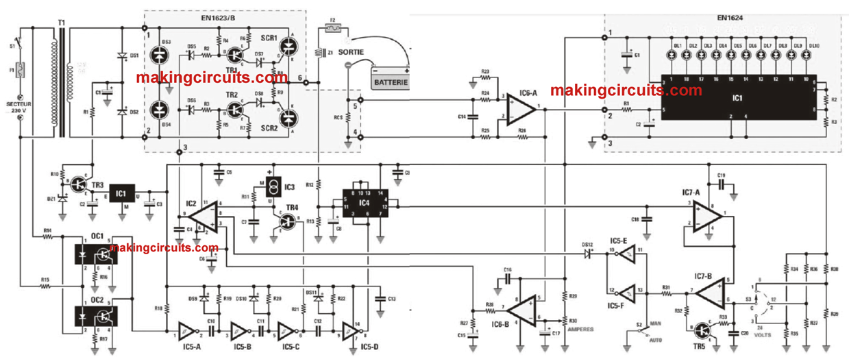
As displayed in the full circuit diagram of this universal 6V, 12V, 24V automatic battery charger circuit for the automobiles, we employ a transformer T1 of 190 VA reducing the stage 230 V to 32 V (additionally of course). The integrated circuits of the control circuit of this battery charger are provided from the voltage rectified by DS1-DS2 smoothed by C1 and stabilized at 33 V by TR3 and the DZ1 attached to its base; The regulator IC1 after that stabilizes it at 15 V. The AC mains signal is identified up by two photocouplers OC1-OC2 to be able to know if the zero crossing of the sinusoidal signal occurs at 50 Hz. This signal is converted In square wave through the gates IC5 / A-IC5 / B-IC5 / C-IC5 / D and the synchronized signal, entering TR4 and IC2 then TR1 and TR2,
As can be seen, DS3-DS4-SCR1-SCR2 form an ideal bridge offering the voltage necessary to charge the battery. The charge level is scheduled through the switch S3 that enables to decide on one of the three voltages 6, 12 and 24 V. Our battery charger is dependent on the specification of varying the charging voltage just by tweaking the conduction time Of the controlled diode and that is the thyristor.
Observe that the thyristor acts similar to a diode but a diode whose current runs between anode and cathode and could be managed by working on the junction through pulses delivered to the trigger.
Throughout the charging of the battery, the voltage can vary in the initial charge level to the voltage value hard-wired employing S3. IC4 is attached as a switch enabling the voltage at the terminals of the battery to move when the mains sinusoid goes by zero phase; Therefore, within this transition to 0, the thyristors tend not to execute and the voltage neglects at IC7 / A, installed in "buffer" (buffer).
The comparator IC7 / B may then evaluate the actual voltage of the battery (status of charge) given by IC7 / A and the voltage determined with S3. If the voltage of the comparator IC7 / B differs from that preferred with S3 then this output 7 of IC7 / B normally takes the logic level 1 and the signal with the two inverters IC5 / E-IC5 / F, driver IC2 that retains As a result the thyristors in conduction to be able to carry on the charge of the battery.
Remember that when the thyristors conduct, the voltage is likely to move into high instant values and, with no large choke Z1 which encapsulates them, the current might also provide such peaks. Z1 acts for the current as a capacitor for voltage.
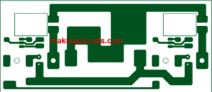
To prevent making use of cumbersome and expensive resistances with low ohmic values on which to sketch a measurable current percentage, we now have drawn directly on the printed circuit a "strip line" RCS. Its functionality is specifically to exchange a resistance of really low value. The charging current is therefore supervised instantly and, appropriately converted into voltage level by IC6 / A, this current is visualized by way of IC1 by means of a luminous scale through a bar of 10 LEDs
The voltage obtained from the RCS terminal is additionally compared with IC6 / B with the voltage extracted from the potentiometer R30 accustomed to alter the load current (from 1 to 5 A).
Once the switch S2 is in the Regular situation, the battery continues to be in the charging state forever, since the IC5 / E-IC5 / F ICs terminate the current control over IC6 / B through the signal delivered to pin 8 of IC2 . While, alternatively, S2 is in the automatic situation, it is IC6 / B that, constantly monitors and controls the current of the battery, adjusts it to match with the chosen current with the
potentiometer R30.
One fuse F2 on the positive output and an additional F1 at the input of the mains supply give you a sufficient assurance against probable short circuits.
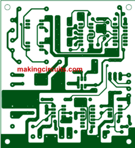
PCB design for the complete 6V, 12V, 24V automatic battery charger circuit.
Parts List
R1 ..... 220 2 W
*R2 ... 1 k
*R3 ... 1 k
*R4 ... 4,7 k
*R5 ... 4,7 k
*R6 ... 220
*R7 ... 220
*R8 ... 1 k
*R9 ... 1 k
R10 ... 1k
R11 ... 470
R12 ... 1 k
R13 ... 1 k
R14 ... 33 k 1 W
R15 ... 33 k 1 W
R16 ... 1 M
R17 ... 1 M
R18 ... 10 k
R19 ... 33 k
R20 ... 10 k
R21 ... 10 k
R22 ... 10 k
R23 ... 180 k
R24 ... 1 k
R25 ... 1 k
R26 ... 180 k
R27 ... 1 k
R28 ... 10 k
R29 ... 10 k
R30 ... 10 k pot. lin.
R31 ... 10k
R32 ... 10 k
R33 ... 10 k
R34 ... 3,3 k
R35 ... 47 k
R36 ... 12 k
R37 ... 10 k
R38 ... 15 k
R39 ... 4,7 k
RCS ... strip line
C1...... 100 μF 50 V électrolytique
C2...... 100 μF 50 V électrolytique
C3...... 10 μF électrolytique
C4...... 1 nF polyester
C5...... 100 nF polyester
C6...... 2,2 μF électrolytique
C7...... 470 nF polyester
C8...... 100 μF 25 V électrolytique
C9...... 100 nF polyester
C10 ... 47 nF polyester
C11 ... 47 nF polyester
C12 ... 100 nF polyester
C13 ... 100 nF polyester
C14 ... 100 nF polyester
C15 ... 10 μF électrolytique
C16 ... 100 nF polyester
C17.... 10 μF électrolytique
C18 ... 1 μF polyester
C19 ... 100 nF polyester
C20 ... 100 nF polyester
Z1...... ZBF1623
DS1........1N4007
DS2........1N4007
*DS3 .....BYW29
*DS4 ..... BYW29
*DS5 .....1N4007
*DS6 .....1N4007
*DS7 .....1N4007
*DS8 .....1N4007
DS9........1N4148
DS10 .....1N4148
DS11 .....1N4148
DS12 .....1N4148
DZ1........zener 33 V 1 W
*SCR1...thyristor TAG675/800
*SCR2...thyristor TAG675/800
*TR1......PNP ZTX753
*TR2......PNP ZTX753
TR3 ........NPN ZTX653
TR4 ........NPN BC547
TR5 ........NPN BC547
OC1........phot. H11AV/1A
OC2........phot. H11AV/1A
IC1 .........LM342/15
IC2 .........LM311N
IC3 .........LM334
IC4 .........CMOS 4007
IC5 .........CMOS 40106
IC6 .........LM358
IC7 .........LM358
T1...........transformateur secteur
190 VA 230 V / 32 V 6 A
mod. T190.01
F1...........fusible 2 A
F2...........fusible 10 A
S1 ..........interrupteur
S2 ..........interrupteur
S3 ..........commutateur 3 positions
Note: components with an asterisk
Are mounted on the power stage
main board. Resistances are
Of 1/4 W unless otherwise stated
For the small board
R1 ..... 10 k
R2 ..... 1,2 k
R3 ..... 680
C1...... 10 μF électrolytique
C2...... 47 μF électrolytique
DL1 ...DL5 ...5LEDs
DL6--DL10---5 Leds
IC1..... LM3914
Note : all 1/4 W.
Final Prototype Image

Complete wiring and PCB connection layout diagram


Friends
How to make Z1…… ZBF1623.
Thanks greetings
Sorry Ivan, I don’t understand what you are saying…where is Z1?
Please send me email reply, i want to build this, but i cannot get the grisp of rcs and i want to also make some additions, which i would appreciate your help with.
sorry, I don’t have any idea about RCS, and where it can be found
Miroslav
I want to make this charger too.
Contact me at email @gmail.com