The transmitter is directly connected to a power outlet, which also provides the necessary energy for its operation. By pressing the control button, the circuit generates a carrier frequency of around 100 kHz pulsed by pulses of approximately 1 kHz. On another power outlet of the installation, a receiving module amplifies these signals and integrates them to ultimately result in a bistable flip-flop acting on a usage relay that directly provides the 220-volt potential of the power grid to power the receiver in question. The system operates according to the principle of a remote switch, namely, alternating between turning on and off with each press of the transmitter's button.
Transmitter Power supply
The power supply, which is activated as soon as the push button is pressed, comes, of course, from the power grid itself via capacitive coupling. Indeed, during a half-cycle which we will qualify as "positive" for the sake of explanation, capacitor C2 charges through C1, R1, and D2.

The potential of the positive electrode of C2 is limited to 12 volts by the Zener diode DZ. During the next half-cycle, capacitor C1 can discharge (or charge in the reverse direction) through R1 via diode D1, in order to be ready to face the next positive half-cycle.
As a result, there is a slightly fluctuating potential of about 12 volts on the positive electrode of C2. The role of R2 is purely safety-related. Indeed, it allows the discharge of C1, which prevents the careless operator from accidentally touching the electrodes of this capacitor and suffering from unpleasant shocks, even if the push button is no longer pressed.
Pulse generation
NAND gates III and IV form an astable oscillator generating non-square wave pulses at their output due to the intentional imbalance introduced by diode D3.
The period of this signal is approximately 750 microseconds, corresponding to a frequency of about 1.3 kHz. The duration of the high states is shorter than that of the low states: about 150 microseconds, which is 20% of the entire period duration.
Carrier Wave Generation
NAND gates I and II also constitute an oscillator, but of the command type. Indeed, it only becomes active when its input 2 is subjected to a high state.
Outside of this situation, the oscillator output is in a permanent low state. During high states, the oscillator delivers a square wave signal characterized by a period of about 10 microseconds, or a frequency of 100 kHz.
Amplification
The signals developed by the two oscillator stages are fed to the base of the NPN transistor T through R8.
On the collector, an amplified and inverted signal is observed. These signals are injected into the 220-volt power grid via capacitor C5.
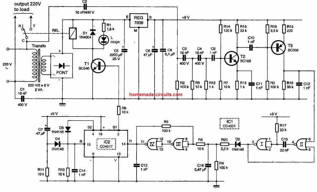
The Receiver Power Supply
The energy comes from the 220 volt sector through a transformer which delivers an alternating potential of 12 volts on its secondary winding. A bridge of diodes rectifies the two alternations and the capacitor C5 provides a first filtering.

On the positive leg of C5, a slightly undulating potential of about 12 to 15 volts is detected, which also directly powers the use relay in case of its solicitation.
At the output of the regulator 7809, a continuous and stabilized potential of 9 volts is observed.
The capacitor C6 provides additional filtering while C8 decouples the power supply of the circuit itself.
Reception and Amplification of Remote Control Signals
The remote control signals coming from the sector are received through the capacitive coupling made up of capacitors C1 and C2.
Afterwards, and after a first treatment carried out by the RC cell formed by the set R2, R6, R12, C3, C4 and C9, the signals are sent to the base of the NPN transistor T2 mounted in common emitter and biased so as to present a collector resting potential equal to about half the supply voltage.
In order to increase the amplification coefficient of this first stage, the emitter resistance R13 is decoupled by the capacitor C11.
Via C10, these signals are then directed to the base of the PNP transistor T3, also mounted in common emitter. Its base is biased so that the collector resting potential is zero.
The capacitor C12 integrates the carrier of the signal so that at the level of the collector of T3, only low frequency pulses are detected.
Signal shaping
The positive 1.3 kHz pulses are taken into account by a monostable flip-flop made up of NOR gates I and II of IC1.
This delivers consecutive high states (with a period of 750 ps) of about 500 ps duration on its output. These high states are then fed to the input of an integrating device formed by the set D2, R20, R4, and C16.
The capacitance C16 charges quickly during the high states through D2 and R20 and can only discharge more slowly during the low states in the higher value resistor R4. This results in a pseudo-high state on the positive electrode of C16.
Subsequently, this high state, which actually corresponds to pressing the reset button, is presented to the trigger input of the Schmitt trigger made up of the NOR gates III and IV and their peripheral resistances R8 and R5.
At the output of the latter, a high state is then detected delimited by very vertical rising and falling edges.
How to Use
The referenced circuit IO2 is a CD 4017. It is a decimal counter-decoder somewhat diverted from its normal role. Indeed, on each positive edge presented on the "Clock" input, the counter advances one step. If a high state is available on the SO output, it moves to the S1 output when this rising edge is presented.
At the following solicitation, the high state moves to the S2 output. But since these are connected to the "Reset" input of the counter by D3, the latter is reset to zero.
Ultimately, the S1 output alternates between a high and a low state at the rhythm of the commands from the reset button.
At the time of receiver startup or after a power outage, for example, capacitance C7 charges through R11. This results in a brief positive pulse immediately sent to the "Reset" input of the counter via D4.
This arrangement thus ensures automatic initialization of the receiver upon startup. As soon as a high state is available on the S1 output, transistor T1 saturates.
It includes in its collector circuit the utilization relay winding. The latter closes. Through its common/NC/NO contacts, the 220-volt AC potential is directly available on the receiver's load output.
The closing of the relay is signaled by the lighting of the red LED L. Finally, diode D1 protects transistor T1 from the effects of self-induced overvoltage that occur mainly during power outages.
Construction
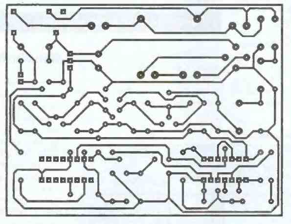
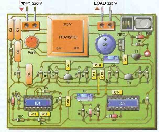
The Figure below shows the printed circuit boards of the transmitter and receiver. There are few remarks to be made on this subject. The usual methods of reproduction will be used.
Particular attention should be paid to the correct orientation of polarized components. The system requires no particular adjustment.
During testing, it is recommended to avoid touching the components, especially at the transmitter level, since the connections of the latter may be directly related to the 220-volt mains and may present a potential of 220 volts relative to ground.


Leave a Reply