The high input impedance and high gain of the FET encourage ease and efficiency in multiple transistorized oscillator circuits. often, the FET can be utilised directly in transistor circuits and needs no unique circuit components. This convenience is vital, particularly in crystal-controlled, RC-tuned, and capacitance-feedback oscillators.
Loading of LC-tuned circuits by the FET which are negligible can cause increased output and decreased distortion than usually received with comparable bipolar transistors. These needed properties also eliminate the need to tap coils for transistor impedance pairing, and incline to maintain the untouched stated of the Q of the tank circuit. The high gain receivable with many FETs makes sure that enough output voltage will be provided for smooth feedback.
FETs are handy in oscillators of all kinds. They can be utilised across the frequency-spectrum which is from low audio frequencies to high radio frequencies. It is noted that the oscillator out can be a symmetrical sinusoidal waveform or a non-sinusoidal pulse.
1) Transformer-feedback AF oscillator
In the figure below, you can see the circuit of an audio-frequency oscillator that utilises inductance-capacitance tuning and inducive feedback and holds a 2N2608 p-channel FET. This standard setup is handy for general-purpose, single-frequency applications, like bridge excitation, tone signalling, signal injection and tracing, and amplifier testing.
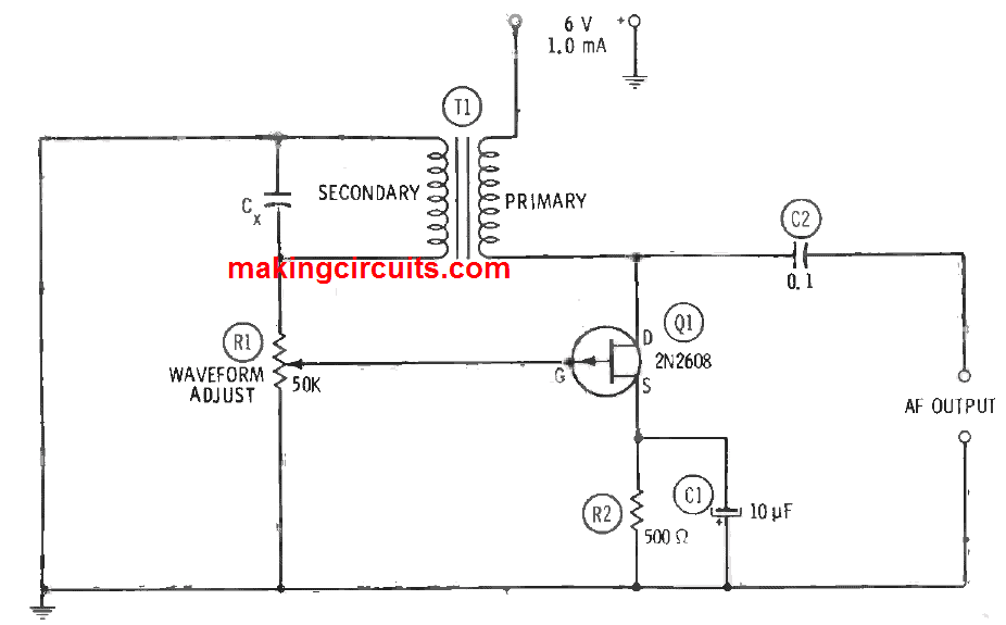
An interchanged audio transformer, T1 delivers feedback from the drain (output) circuit to the gate (input) circuit. It has s 2:1 (or more) step-up turns ration between primary and secondary windings. This transformer must be polarized accurately for regenerative feedback by good primary and secondary connections.
Capacitance Cx, sets the oscillation frequency and the inductance of the secondary of the transformer:
f = 1 / (2π √LC)
Where,
- f = oscillation frequency in Hz
- L = inductance of the transformer secondary in henrys
- C = capacitance of Cx in farads
Because the transformer producers do not normally specify the winding’ inductance, we have to measure this value, or diverse capacitors may be examined as Cx until the needed frequency is obtained. Because of the self-capacitance of the secondary oscillation will happened at one frequency when no external capacitor is in the circuit, and this is the maximum frequency at which the circuit will function.
The feedback amplitude is regulated with a potentiometer R1, which must be configured for best sine-wave output shown by an oscilloscope attached to the AF OUTPUT terminals. Extreme feedback overdrives the FET and locks the output-wave peaks; inadequate feedback will result in instability and sluggish commencing.
A U.T.C. Type S-8 transformer evaluated in this circuit provided a frequency of 500 Hz with Cx = 0.002 µF, and 1.1 kHz with no external capacitor. At 500 Hz, the open-circuit output voltage was 1 Vrms and the current drain is 1 mA at 6 VDC. It is possible to commence comparable operation with some of the smaller, transistor-type transformers.
Because the output is capacitance coupled from the drain circuit which contains transformer t1, the external load will deliberately detune oscillator to some degree. This effect can be removed by including a source follower to isolate the oscillator from the load. The gate electrode of the 2N2608 is internally attached to the metal container of this FET, so it is crucial to be cautious when mounting the FET to avoid contact between the container and other components or wiring. The ratings of resistor R2 and electrolytic capacitor C1 is 0.5 watt and 25 dcwv respectively.
2) LC-tuned AF Oscillator
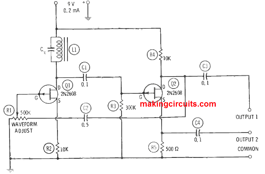
As depicted in the following figure, the frequency is decided by capacitance Cx, and the inductance of iron-cored inductor L1:
f = 1 / (2π √LC)
Where,
- f = oscillation frequency in Hz
- L = inductance of the transformer secondary in henrys
- C = capacitance of Cx in farads
On this circuit, L can be obtained from any convenient coil (from a filter choke to a high-Q adjustable inductor), and Cx may be chosen to provide a desired frequency. You may begin with a standard coil and choose a capacitor or commence with any simple capacitor and select an inductor.
The circuit is 2-stage RC-coupled amplifier, containing 2N2608 FETs, with the tuned circuit (LCx) creating the plate tank of the first stage and with comprehensive feedback for oscillation delivered by capacitor C2. An even number of stages is obligatory for the required positive feedback. Potentiometer R1 permits the feedback amplitude to be regulated for best sine-wave output, as witnessed with an oscilloscope attached to the output terminals (either OUTPUT 1 or OUTPUT 2). Extreme feedback overdrives Q1 and disrupts the output wave; inadequate feedback causes instability and sluggish starting.
With L1 = 5H and Cx = 0.005 µF, the frequency is 1 kHz. The open-circuit signal voltage at OUTPUT 1 (high-impedance output) is 1 Vrms, and OUTPUT 2 (low-impedance output) is 0.6 Vrms. Current drain here is 0.2 mA at 9 VDC. It is very important to keep all wiring short, direct and rigid for maximum stability and minimum stray pickup. Moreover, the whole device must be case shielded. The gate electrode of the 2N2608 is internally linked to the metal case of this FET. Therefore, exert caution to avoid contact between the FETs and other components in the circuit. All the fixed resistors R2, R3, R4 and R5 are rated 0.5 watts.
3) Phase-shift AF Oscillator
The phase-shift oscillator is famous for its superb sine wave output and the flexibility and compactness of the resistance-capacitance network that decides its frequency. In figure below, you can see the FET version of this known circuit which contains a single 2N4338.
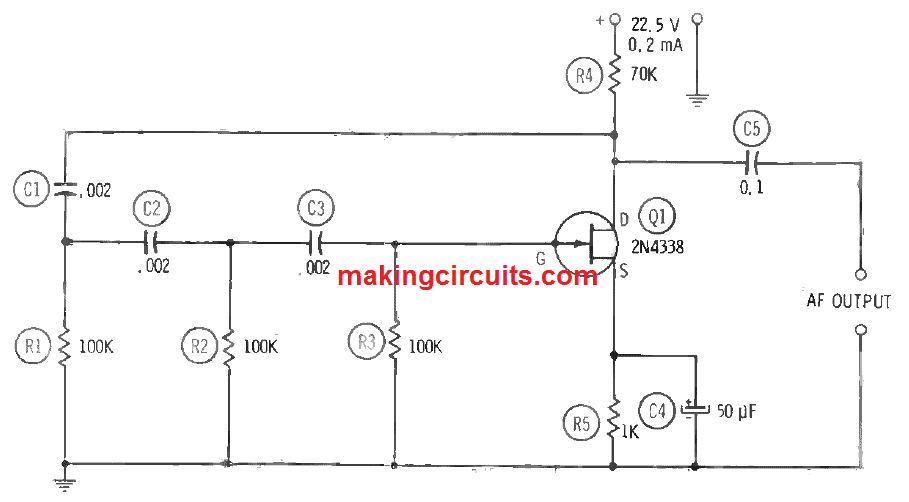
The frequency-deciding RC network comprises exact capacitors C1, C2 and C3 and similar resistors R1, R2 and R3. Each leg of this network (C1-R1, C2-R2 and C3-R3) generates a 60-degree phase shift. Eventually, a complete 180-degree phase shift initiated in the feedback path from drain to gate of 2N4338 is right for the positive feedback required for phase angle of each leg of the network is 60 degrees.
f = 1 / 10.87 RC
Where
- f = frequency of oscillation in hertz
- R = resistance of R1, R2 or r3 in ohms
- C = Capacitance of C1, C2 or C3 in farads
Equating the formula, we are left with C = 1/(10.87fR) and R = 1/(10.87fC). Make sure to choose the capacitors and resistors rating at 1 percent or better accuracy. The network values shown in Figure 3.3 (C1 = C2 = C3 = 0.002 µF, and R1 = R2 = R3 = 100 kΩ) deliver a signal frequency of an estimated 460 Hz. The open-circuit output voltage of the circuit at this frequency is 8 Vrms. Current drain is 0.2 mA at 22.5 VDC.
In this single-stage circuit, the FET must be a strong amplifier (where its transconductance must be high), or the result will be zero oscillation. Particularly, the voltage boost of the circuit must be adequate high to override the insertion loss of the RC network. Otherwise, the feedback voltage meeting the gate will not be enough to promote oscillation. Likewise, in standard oscillators, the output in this circuit is capacitance coupled from the drain circuit which contains the input end of the phase-shift network. Due to this, the external load may appear to detune the oscillator a little. This flaw can be rectified by including a source follower to isolate the oscillator from the load.
As always, it is fundamental to keep all wirings short, rigid and direct for all-out stability and least stray pickup. Though, total shielding is not needed unless the oscillator is utilised in an environment of strong magnetic fields. Nevertheless, you must exert caution to mount the 2N4388 clear of other components and wiring, as the gate electrode is internally linked to the metal enclosure if this FET and is susceptible to capacitive pickup in addition to short circuits and grounds. All the resistors used in this setup are rated 0.5 watts while the electrolytic capacitor C4 is rated 25 dcwv.
4) Single-frequency Wien-bridge AF oscillator
Wien-bridge is another type of RC-tuned audio oscillator which is commonly used. The circuit is quite straightforward than the phase-shift oscillator mentioned in the preceding section. This is because the Wien bridge utilises only two resistors and two capacitors to assign the frequency whereas the phase-shift oscillator needs three capacitors and three resistors. Ultimately, the Wien-bridge circuit demands two FETs.
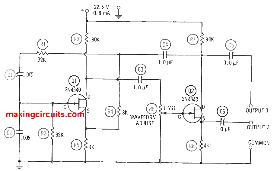
Figure above displays a Wien-bridge oscillator circuit configured for single-frequency audio operation. This circuit which holds two 2N4340 FETs (Q1 and Q2) is a two-stage RC-coupled amplifier with a Wien bridge (C1, C2, R1 and R2 worked against R4 and R4) attached in the feedback path from the output drain (Q2) to the input gate (Q1). In this frequency-deciding RC network, C1 = C2, and R1 = R2. At a specific frequency chosen by these R and C values, the feedback voltage at the Q1 gate is in the proper phase for oscillation. Moreover, all other frequencies degeneration generated by the feedback-voltage drop across the sum of R4 and R5 cancels oscillation. As a result, the output of the Wien-bridge oscillator has a fantastic sinusoidal waveform. When C1 = C2, and R1 = R2,
f = 1 / 2πRC
Where,
- f = oscillation frequency in hertz
- R = resistance of R1 in ohms
- C = capacitance of C1 in farads
Rearranging the formula, we get C1 = 1/2 fR and R1 = 1/2 fC. The values of C1, C2, R1 and R2 provided in Figure 3.4 are correct for 1 khZ operation. A very good sine-wave output is gained at this frequency when potentiometer R6 is configured for the OUTPUT 1 and COMMON terminals. The zero load output yields 6 Vrms at the OUTPUT 1 (high impedance) terminal, and 0.4 Vrms at the OUTPUT 2 (low impedance) terminal. The current drain is 0.8 mA at 22.5 VDC.
For peak stability and minimum stray pickup, it is important to ensure the wirings are short, steady and direct. Since, the gate electrode of 2N4340 is internally connected to metal enclosure of this FET, both transistors must be mounted clear of other components. The fixed resistors are rated 0.5 watts. Due to the high output being capacitance coupled from the Q2 drain circuit which is coupled to the Wien-bridge network through capacitor C4, the output load may incline to detune the oscillator a little. However, this disruption can be rectified as suggested for the phase-shift oscillator, by including a source follower to isolate the oscillator from the load.
5) Drain-coupled Multivibrator
In figure below, a circuit of a free running multivibrator, founded on two 2N4340 FETs (Q1 and Q2) is shown. This setup is the same as the plate-coupled, BJT multivibrator.
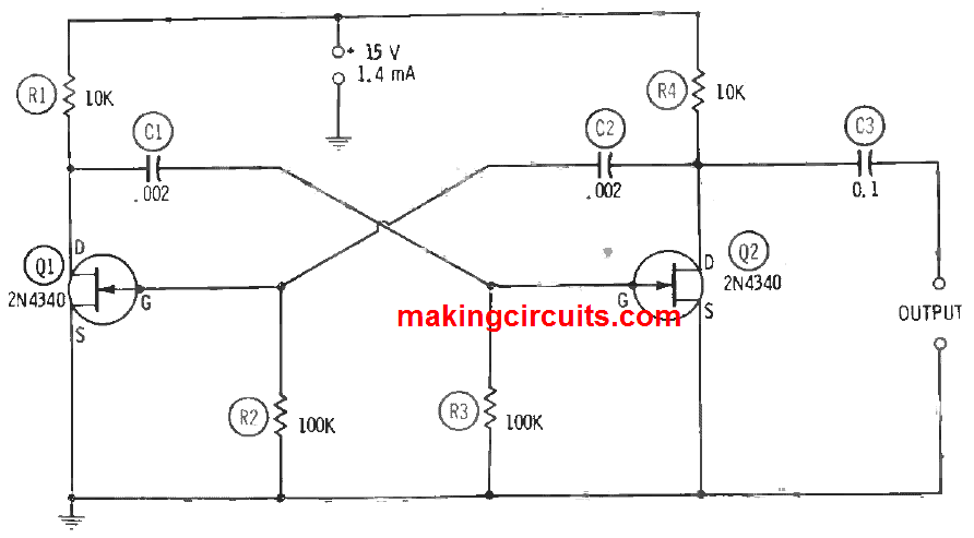
Basically, the multivibrator is an RC-coupled amplifier with the output of each of the two stages powering the input of the other. So, as depicted in Figure 3.5, the drain of Q1 is coupled through capacitor C1 to the gate of Q2, and the drain of Q2 is couple across capacitor C2 back to the gate of Q1. Like in the BJT circuit, the frequency which is produced is controlled by the time constants of the cross-coupled RC legs where capacitances are measured in farads and resistances in ohms. If the components are carefully paired (C1 = C2, and R2 = R3), the equation becomes
f = 1 / (C1R3 + C2R2)
The coupling resistance and capacitance values shown in Figure 3.5 provide 2.5 kHz operation. Some modifications of these values may be needed with individual FETs. The output signal is a rectangular wave consisting a zero-load amplitude of 12 V peak-to-peak when a 15-V DC supply is utilised. Current drain is 1.4 mA and synchronising signal may be channelled at either gate or drain.
Resistors R2 and R2 must be the close to 1 percent or better, and so as the capacitors C1 and C2. All resistors are rated 0.5 watts. The wirings for this circuit, as others, must be maintained short and rigid. However, lead dress not crucial except when operating at 5 kHz and higher. The 2N4340s should be installed out of contact with each other or with other components, since the gate electrode is internally linked to the metal case in this FET.
6) Source-coupled multivibrator
The circuit shown in Figure below is a simpler free running multivibrator network compared to preceding circuits. This source-coupled multivibrator is equal to the emitter-coupled, BJT circuit.
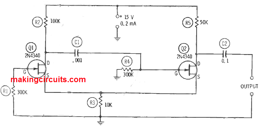
In this configuration, utilising two 2N4340 FETs (Q1 and Q2), only one interstage coupling capacitor (C1 in the forward path from Q1 to Q2) is required. The coupling back from the second FET (Q2) to the first (Q1) is attained by the common source resistor, R3.
The produced frequency relies fundamentally on capacitance C1 and resistance R4. The C1 and R4 values displayed in Figure 3.6 are exclusive for 550 Hz operation. Elevate C1 for lower frequencies and decrease it for higher frequencies. The output is a rectangular wave with an amplitude of 10.5 V peak-to-peak when the DC supply is 0.2 mA at 15 VDC. A synchronised voltage may be channelled at the gate of Q1.
The resistors in this setup is 0.5 watts and like in the previous circuit, the wirings must be maintained short and rigid. Lead dress is not importance except when utilising frequencies of 5 kHz and higher. The 2N4340s must be installed free from contact with each other or with other components, since the gate electrode is linked within to the metal case in this FET.
7) Self-excited RF oscillator
The 2N3823 FET has incredible high-frequency figure of merit (ratio of transconductance to input capacitance). Therefore, it is handy for RF applications through the VHF area. A circuit of self-excited radio-frequency oscillator having this FET is displayed in the figure below.
This is a series-fed Hartley circuit where the tank circuit L1-C1 decides the produced frequency. The values of C1 and L1 can be found for a desired frequency, either in terms of an available capacitance or available inductance.
C1 = 1 / 39.5f2L1
L1 = 1 / 39.5f2C1
Where,
- C1 = capacitance in microfarads
- L1 = inductance in microhenry
- f = frequency in megahertz
The inductance and capacitance values can be determined with the assistance of a reactance slide rule of l-c-f chart. For variable frequency operation, either C1 or L1 may be regulatable. The coil is centre tapped, but in some cases the tap may need to be moved away from the centre. Radio frequency output may be capacitance coupled from the drain, as depicted in the following figure. In this instance, the zero-load RF output amplitude is 2.5 Vrms when the DC input is 5.3 mA at 6 VDC. From a classical approach, you can use link couple out of L1. The RF potential across L1 is 1.3 V peak.
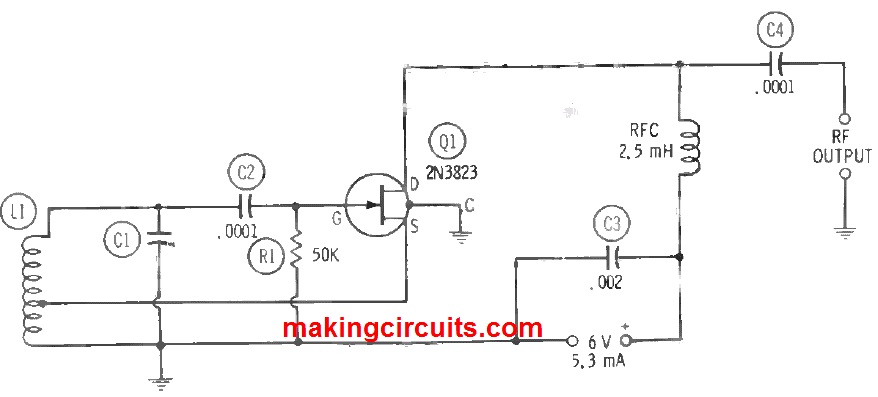
In all circuits similar to this, the wirings must be maintained short, direct and rigid particularly at frequencies above 1 MHz. The enclosure of 2N3823 is linked to a fourth pigtail which must be grounded as displayed. The resistors used in this circuit are rated 0.5 watts.
8) Conventional Crystal Oscillator
A circuit of a crystal-controlled RF oscillator containing a 2N3823 FET is shown in Figure below. The circuit is same to the classic collector tuned, BJT-type circuit and is worked in the fame manner as the latter.
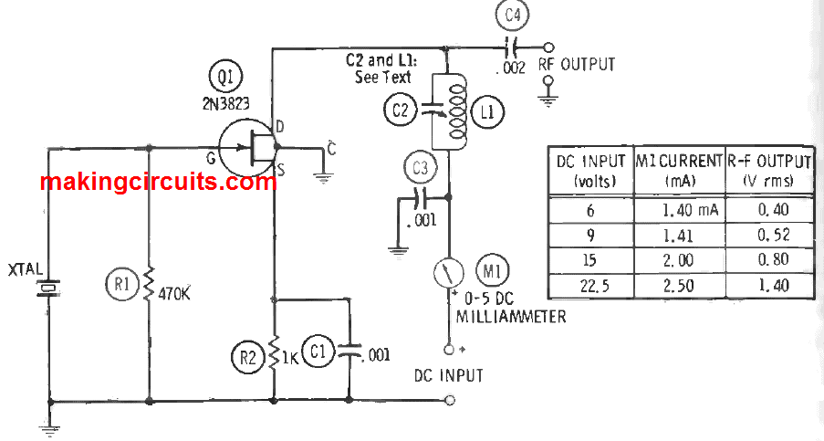
In this setup, capacitance C1 and inductance L1 are selected to resonate at the crystal frequency. These tank-circuit values may be decided for a wanted frequency either in terms of a free capacitance or inductance:
C2 = 1 / 39.5f2L1
L1 = 1 / 39.5f2C2
Where,
- C2 = capacitance in microfarads
- L1 = inductance in microhenry
- f = frequency in megahertz
The inductance and capacitance may be assigned with some assistance from the reactance slide rule or l-c-f chart. Either C2 or L1, or both, may be made regulatable. The circuit is configured to the crystal frequency in the conservative manner. This is done by tuning either C2 or L1 for drain-current dip designated by DC milliammeter M1. Figure 3.8 depicts the zero-load RF output voltages achieved with diverse values of DC supply voltage and current. A standard capacitance-coupled RF output is displayed in Figure 3.8. Still, energy may also be inductively coupled out of the oscillator, using a link coil attached to the lower end of the coil L1.
All wirings must be ensured short, direct and rigid. The setup of 2N3823 is attached to a fourth pigtail which must be grounded as shown in the figure. The pair of resistors are rated 0.5 watts. The best high-frequency performance, C1, C3 and C4 must be mica capacitors. If C2 is attached, it must be of silvered mica.
9) Pierce Crystal Oscillator
The Pierce crystal oscillator is simple to use because it usually requires no tuning. This circuit is conveniently used in calibrators, marker generators, crystal-testing oscillators and radio transmitters. Figure below displays a Pierce circuit and the voltages are achieved with diverse values of DC supply. This is a robust oscillator.
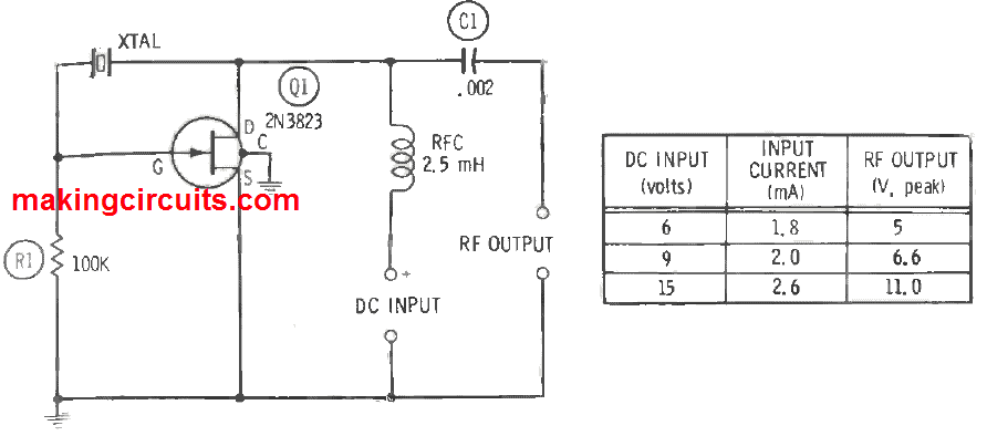
The operator must be used to with the kind of crystal he or she utilises in this circuit as the Pierce oscillator is more inclined to the fundamental frequency. Harmonic-type crystals function here at their fundamental frequency only.
Like all circuits in this section, the wirings must be kept short and rigid. The case of the 2N3823 is linked to a fourth pigtail which must be grounded as shown. Resistor R1 is 0.5 watt, and capacitor C1 must be a mica unit.
10) 100-kHz Crystal Oscillator
A 100-khZ crystal oscillator is treasured when it is used a frequency standard and crystal calibrator. Figure below displays the circuit of a standard oscillator of this kind having a 2N3283 FET, which needs zero tuning. The circuit is a quick starter and robust oscillator.
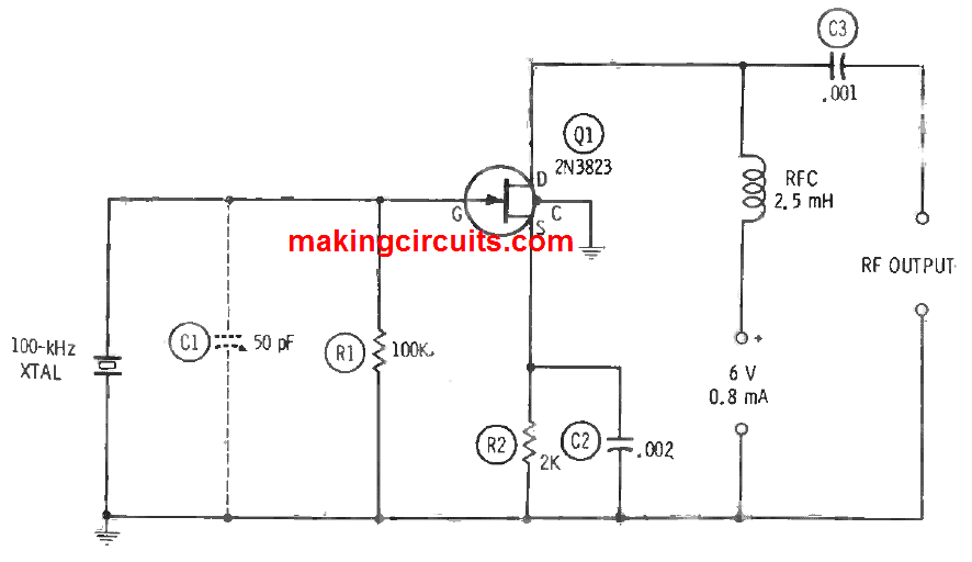
At 6 V, 0.8 mA DC input, the zero-load RF output is 5.4 Vrms, and this output is adequately nonsinusoidal that the 100-kHz harmonics may be recognized deep into the radio-frequency spectrum. If the oscillator frequency is to be configured against standard frequency signals from WWV or some other standard, the non-compulsory air trimmer capacitor C1 can be included. A 50-pF unit should permit the crystal frequency to be moved just enough for the zero beating of a suitable harmonic with the high-frequency standard signal.
All wiring must be maintained short, direct and rigid. The metal contained of the 2N3823 is attached to a fourth pigtail which could be grounded as depicted. Resistors R1 and R2 are rated 0.5 watts, and C2 and C3 are mica capacitors. (The capacitance of C3 could be lessened in some setups to limit loading of the oscillator. In all cases, coupling must be as loose as possible.)
11) Colpitts AF Oscillator
The Colpitts oscillator has the edge that its inductor required no tap, and no transformer is needed for feedback. Despite the simplicity, the oscillator can produce a good output waveform and will function at radio and audio frequencies. Figure below displays the circuit of a Colpitts AF oscillator. In basis, this is a single-frequency unit (900 Hz) but the frequency may be dispersed over a thin range (650-900 Hz) if a slug-tuned 5-henry inductor is utilised as shown below. The oscillator is designed around a single plastic-covered FET (Q1). DC drain is 0.5 mA at 9V, and the related no-load output signal is 4.5 Vrms. With assistance from an oscilloscope or distortion meter linked to the AF OUTPUT terminals, rheostat R2 can be configured for most feasible sine waveform.
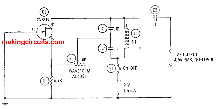
The frequency may be altered by replacing other values for the C1 and C2 values, but the 10:1 ratio must be maintained between C1 and C2. A slight frequency shift may be attained, when a steady inductor is applied for L1, by differentiating only one capacitance. For instance, if L1 = 5 H and C2 is swapped to 0.07 µF, the frequency changes to 1 kHz. It must be remembered rheostat R2 must be regulated for the best output waveform.
Source resistor used in this experiment is rated 0.5 watts. The frequency-determining capacitors C1 and C2 must be high-grade units for stability and have good waveform. (As mica is desirable, such capacitors are costly in the big capacitances used here where decent plastic units are good enough.) The output coupling capacitor C2 is a 100-V plastic unit.
12) Code-practice oscillator
Figure below shows the code-practice as seen in the application of the Colpitts circuit of the previous section. In this device, magnetic headphones deliver the inductance of the frequency-deciding circuit.
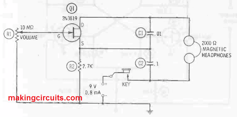
Therefore, you wouldn’t need another coil or transformer. This oscillator that provides a heavy signal (a maximum output of 4.2 Vrms is produced across a pair of Trimm 2000-ohm magnetic headphones). Current drain is 0.8 mA at 9 VDC.
Using the Trimm phones and C1 = 0.01 µF and C2 = 0.1 µF, the signal frequency is around 1 kHz. This can be modified by changing the C1 and C2 values while maintaining their 10:1 capacitance ratio. Still, limited frequency difference may also be attained without eliminating oscillation, by varying only C2. The lower the capacitances, the higher the frequency is, and vice versa.
The oscillator engages smoothly and has a decent clear tone. The headphone volume may be changed with only little effect on the frequency and waveform from a 10-megaohm rheostat R1. As there is zero current unless the key is actuated, an on/off switch will not be necessary. Resistor R2 is rated 0.5 watts in this experiment. The quality of capacitors C1 and C2 is not important in this setup, so both capacitors may be of any type that is suitable for the user. However, if frequency stability and unmistakable waveform are required, C1 and C2 must be made of decent-grade 100-V plastic units.
13) Flip-flop
Figure below depicts a classic, drain-triggered flip-flop circuit containing two HEP F1036 FETs (Q1 and Q2). This setup draws only about 15 µA from the 18-V DC supply.
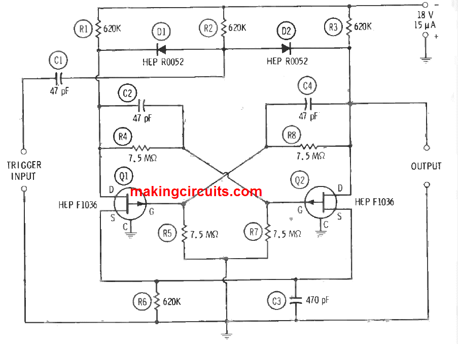
Be it the circuit exhibits a slow switching speed that is restricted to upper audio frequencies, still it explores many applications in control systems, low-speed counters and memories where high speed is not required.
A 9-V pulse delivered to the TRIGGER INPUT terminals will activate the flip-flop in accordance with its previous state. The on output is around 9 V, given non-load conditions at the output terminals. For optimum results, a matched pair of FETs (Q1, Q2) and similar diodes (D1, D2) must be used. In the same manner, identical resistor values must be matched. Finally, even the commutating capacitors (C2, C4) must be exact.
Thanks, this is all very useful! I will get to building and testing
Thank you!!
impossible to see schematics !!!!
cdlt
ln
Please check it now!
its ok !!