Now we have got a very useful programmable timer circuit that we can use for switching some load ON and OFF, but the best thing is that we can do this with two separate delay timings, that we can program independently. So we can set one time delay for switching ON and another different delay for switching OFF and we can set these timings anywhere from 2 seconds to 24 hours then this is why it becomes so useful.
Now we can adjust these ON and OFF delay timings exactly the way we want then, this makes the circuit very flexible. The ON delay and the OFF delay both can be separately adjusted then this becomes the most interesting and the most important feature of this programmable timer circuit.
Using Versatile IC 4060
Right here in this discussion, we will see a very simple but also quite useful timer circuit diagram that we can configure with ON time and OFF time settings, that we can adjust independently, but we can do this using just ordinary potentiometers, then this makes things much easier for us.
So the reason why this circuit becomes so easy to build and configure is because of the IC 4060, that is a very versatile chip and this IC does not need too many components for getting the whole thing working, this makes it a very good choice.
If we see the circuit diagram below then we can find that here, we are using two IC 4060s and both are wired in such a way that they work as two independent timers but there is something to note, that although these two timers are set up separately, they are actually interconnected with each other, that is because their starting operation is linked together.
So basically, both these circuits are designed in the same way and they are arranged in the standard counting mode, that is available in the IC 4060 itself.
How the Circuit Functions
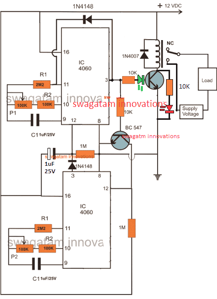
Now we have to understand, how this whole thing is actually working, then we can see that the output of the first IC at the top is connected to the reset input of the second IC at the bottom through a transistor so what this does is whenever the upper IC finishes its timing and its output becomes HIGH then it switches ON the lower IC and forces it to start operating.
Now once the lower IC starts running then, it begins its own timing cycle but now when the lower IC also finishes its own timing and its output becomes HIGH then it stops the upper IC from running and forces it to reset back to its original state, this causes the whole process to start again from the beginning.
So in simple words, we can say that as long as the first IC is running and its time delay is not over then the second IC will remain in standby and will not work, but as soon as the first IC completes its timing and its output goes HIGH, it will activate the load and at the same time it will also start the second IC.
Now we have two potentiometers here, one with the upper IC and one with the lower IC. The pot that is connected with the upper IC can be used for deciding how long we want the load to remain OFF before it turns ON but the pot that is connected with the lower IC will decide how long the load should remain ON before it switches OFF again.
Calculating RC Timing Components
Now we have to see how to set up the delay timing, this can be done by using a formula, but the best way is to do it manually because that is much simpler and also more accurate, then we will follow the manual way, as explained below:
First we have to take any random resistor that is above 100K and connect it in place of P1/R2 in the upper circuit.
Then we will switch ON the circuit and carefully note how much time it takes for pin#3 of the upper IC 4060 to become HIGH. Now this time duration will be our "sample delay".
Once we have noted this delay time, then we can use the following simple cross-multiplication method to calculate the required resistor value for getting any other desired delay time:
Sample Delay / Desired Delay = Selected Resistor / Unknown Resistor
Now let us take an example:
Suppose we find that pin#3 of the upper IC becomes HIGH after 300 seconds, then this means that our sample delay is 300 seconds.
Now we also know what resistor value was used to get this delay, so we can use this value to calculate the required resistor for any other delay time.
For example if we want the delay to be 1 hour or 3600 seconds, then we can put the values in the formula like this:
300 / 3600 = 100K / x (unknown resistor)
Now if we solve this equation, then we get:
300 × x = 360000
x = 1200K or 1.2 Meg
So, now we understand that if we replace P1/R2 with a 1.2 Meg resistor, then we will get a delay of exactly 1 hour at pin#3 of the IC 4060.
But we must remember that this calculation is just an example, then the actual values may be different in real conditions, so we must always check and confirm by testing the circuit manually.
How to Build
Now if we want to make this circuit then we have to follow some simple steps one by one but now we must make sure that we do everything properly otherwise some mistake may happen and then the circuit may not work correctly. So now let us go step by step
Step 1: Gather All Components
First we need to collect all the required parts then we must check each component properly to confirm it is the right one. Now here is what we will need
- Two IC 4060
- Two P1 and P2 pots 100K each
- Resistors 2M2 two pieces 1M three pieces 100K two pieces 10K one piece
- Capacitors 1uF 25V two pieces C1 11uF 25V two pieces
- Diodes 1N4148 two pieces 1N4007 one piece
- Transistors BC547 two pieces
- Relay 12V SPDT
- Load any AC or DC device that we want to control
Once we have all these parts ready then we can move on to the next step.
Step 2: Prepare the Circuit Board
Now we need a PCB printed circuit board or a general purpose perforated board for assembling this circuit but if we want then we can also build it on a breadboard for testing first.
If we are using a PCB then we must check the tracks and clean them properly.
If we are using a perfboard then we must plan where we will place each component.
Now we should mark all the positions of the components on the board so that we do not get confused later.
Step 3: Solder the IC 4060 Chips
Now we will start by fixing both IC 4060 chips onto the board but before that we must make sure the pins are not bent. Then we must insert them in the correct orientation otherwise the circuit will not work.
The notch or dot on the IC must match the diagram.
Once we insert the ICs we must solder them properly without shorting any pins.
Now after soldering we should check with a multimeter to confirm there is no short circuit between adjacent pins.
Step 4: Connect the Resistors and Capacitors
Now we have to add all the resistors and capacitors one by one.
First we take the 2M2 resistors and connect them with P1 and P2.
Then we take the 100K resistors and solder them at the correct places.
Now we place the 1M resistors making sure they go to the right positions.
After this we take the 10K resistor and solder it near the relay section.
Now we take the capacitors 1uF and 11uF and fix them at the right places making sure the polarity is correct otherwise the circuit may not work properly.
Step 5: Add the Diodes and Transistors
Now we will install the diodes and transistors carefully.
First we take the two 1N4148 diodes and solder them correctly making sure their cathode and anode are in the right direction otherwise the circuit will fail.
Then we take the 1N4007 diode and place it near the relay coil for back emf protection.
Now we take the BC547 transistors and fix them at the correct locations but here we must be careful because the pin positions collector base and emitter must be correct otherwise the circuit will not function.
Step 6: Fix the Relay and Output Load Section
Now we will install the relay which will control the external load.
First we take the 12V relay and solder it in the right place.
Then we take the 10K resistor and place it near the transistor that is driving the relay.
Now we connect the output terminals of the relay to the external load making sure the wiring is correct.
The common terminal of the relay must be connected to the supply voltage of the load.
The normally open NO terminal will be connected to the load so that when the relay activates the load turns ON.
Step 7: Make the Power Supply Connection
Now we have to connect the 12V and ground wires to power the circuit.
We take the 12V wire and connect it to the circuits power input.
Then we take the ground wire and connect it to the circuits ground point.
Now we must check everything once to make sure the wiring is correct before switching ON the power.
Step 8: Test and Adjust the Timer
Now we are ready to test the circuit and adjust the timing.
We switch ON the circuit and observe the operation.
The first IC should start counting and after the set delay its output should turn HIGH activating the second IC.
The second IC should then start counting and after its set delay it should switch OFF the relay and reset the cycle.
If the timing is not correct we adjust P1 and P2 until we get the desired ON and OFF durations.
Step 9: Final Check and Installation
Now once everything is working fine we can fix the circuit inside an enclosure to protect it from dust and damage.
We can use a plastic or metal box to cover the circuit.
We must ensure there are ventilation holes to prevent overheating.
The relay output wires should be properly insulated to avoid short circuits.
After this we can connect any device to the relay output and use the timer for automatic switching based on our programmed delay settings.
Hello,
I really like your timer circuit. Could you please also share a version of the schematic where the timer runs continuously (repeating cycles without stopping)?
Thank you in advance!
David
Thanks David,
The circuit explained in the above article will keep repeating non-stop as long as it s powered.