In this post we are going to understand how a phase shift oscillator works and we will be constructing one and also simulate output the using software simulation tools.
Phase shift oscillator is a sine wave oscillator which generates the frequency based on connected resistors and capacitors network. The advantage of phase shift oscillator is good stability and can provide distortion less frequency generation with wide range of loads; however for huge loads we may need pre-amplification stage.
The phase shift oscillator has 3 parts, the RC network, amplifier and positive feedback. Let’s look into them in detail.
The RC network consists of resistors and capacitors connected in ladder form, as shown in figure.
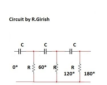
It has three RC stages, each RC stage shift the input frequency by 60 degree. The first stage shifts frequency by 60 degree, second stage shifts frequency by 120 degree and third stage shifts frequency by 180 degree.
The next stage is amplifier, which can be a transistor based amplifier or operational amplifiers. The amplifier stage generates 180 degree phase shift, which gets input from the RC network. So combining both phase shift from RC network and amplifier’s phase shift 180 + 180 = 360 degree.
To get the frequency from the circuit consistently, we need to provide positive feedback to the circuit. There are two types of feedback, positive and negative feedback. Here is general meaning of those:
Negative feedback is feeding the output signal to the input with 180 degree phase shift.
Positive feedback means feeding the output signal to input with zero degree phase shift. In this phase shift oscillator we provide positive feedback.
Simple Phase Shift Oscillator circuit using a single transistor:
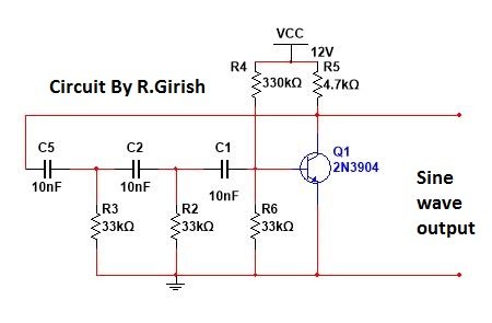
The complete circuit of a simple phase shift oscillator using just a single transistor is given above with explained 3 main parts.
The frequency can be determined by following formula:
Frequency = 1 / 2 x pi x R x C x sq. Root (2N)
Where R is the resistor in Ohms
C is the capacitance in Farads
N is the number of RC stage, N=3
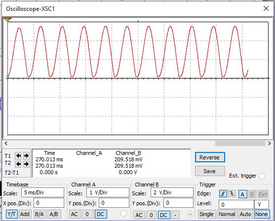
Here is the simulated output:
The operation of the Phase Shift Oscillator is very important because it has never been described before and the only vague reference has been by a Professor who waves his hands around and says something like three phase sections produce 180° Phase Shift.
But no explanation has been provided for this Gobbledygook.
The operation of the Phase Shift Oscillator is very complex and is nothing like you have been told. Forget everything you have learned. .
The first thing you have to understand is the behaviour and operation of a capacitor when it is not connected to either power rail.
It rises and falls in the circuit and when it charges and discharges, you can think of it as increasing and decreasing in length.
When it is connected to a resistor, the voltage across the resistor depends on the charging current of the capacitor.
A capacitor has energy or “charge” in the form of a voltage across its terminals and a current capability according to the number of plates in the capacitor (its capacitance).
The base of a transistor cannot rise above the emitter by more than 0.7v.
When the voltage is below 0.7v, the base is seen as having a very high input impedance, by the rest of the circuit.
When it sees a voltage of 0.7v, any extra voltage delivered to the base will be converted to a CURRENT. A transistor only works on CURRENT. It is difficult to measure current and so we talk in terms of voltage.
When it sees 0.7v, it immediately has a low resistance and only accepts CURRENT.
Increased current makes the transistor turn ON more and the collector voltage falls.
This has never been described before and you will not be able to understand the operation of the Phase Shift Oscillator without this knowledge.
The principle of operation of the Phase Shift Oscillator is to deliver a signal from the output to the base.
A rising signal on the base produces a falling signal on the collector.
This does not produce oscillation. This is called NEGATIVE FEEDBACK.
We want POSITIVE FEEDBACK.
We want a rising signal from the collector to deliver a rising signal to the base to increase the amplitude and maintain oscillation.
An oscillator of this type is actually turned ON more and more until it cannot be turned On any more and then turned OFF until it cannot be turned off any more.
We need a rising signal on the collector to become a falling signal on the base.
In other words, the the rising signal has to turned into a FALLING signal.
This will turn the transistor ON more and more to produce our wave.
We will start with the capacitors fully discharged and no voltage on the base.
This effectively means the transistor is out of circuit and the collector LOAD resistor pulls the 3 capacitors HIGH. The third capacitor is connected to the base and when it sees 0.7v, the transistor gets turned ON a lot and the collector pulls the LOAD resistor down to a very low voltage that just allows the base to see 0.7v.
This means the transistor is not fully turned ON and the collector voltage is slightly higher than 0.7v.
The capacitors now starts to charge and the current into the base reduces.
This allows the transistor to turn OFF slightly and the collector voltage rises.
It is the rate of charging of the capacitors via the two 10k resistors that controls the current into the base.
As they charge, the charging current reduces and you have to understand that the base creates a resistance when its voltage is above 0.7v and it detects this reducing charging current.
There is a fight between the base receiving current and the transistor turning off as the capacitors charge, and this takes a long time and produces the wave from the lowest value to the peak.
Eventually the capacitors are fully charged and the base receives no current and the output is a maximum.
It would remain in this HIGH state if were not for the 1M base-bias resistor.
The left lead of each capacitor is charged to a positive voltage compared to the right-hand lead.
This makes the left lead of the third 22n more positive than the other lead.
When all the capacitors are charged, the voltage across the 10k resistors becomes zero.
This means the right lead of the third 22n is slightly negative and this is what the base sees.
But when the base is below 0.55v it has a very high impedance and the voltage on the third 22n does not change.
The 1M base-bias resistor is connected to this point and it delivers a current to DISCHARGE the third 22n and gradually charge it in the opposite direction until the base sees 0.7v.
This turns ON the transistor and the collector voltage reduces.
This starts to discharge the first two 22n capacitors and reduces the voltage on the base, via the third capacitor.
At the same time a negative voltage is developing across the two 10k resistors. The 1M charges the third 22n in the opposite direction and there is a fight between the first two 22n capacitors getting discharged and the third 22n getting charged.
The collector voltage is reducing and the 1M is having less and less effect and that’s why it is taking longer and longer. But the negative voltage across the second 10k resistor is reducing and this is raising the third 22n to deliver more current to finalise the turning-ON of the transistor.
Eventually the transistor is turned ON with a collector voltage of a little more than 0.7v.
The capacitors are uncharged and the 1M is not capable of keeping the transistor turned ON to this amount. The third capacitor passes its charge to the transistor and it starts to turn OFF.
This raises the collector voltage and via the three capacitors the base sees more current and this stops the collector voltage rising.
But the capacitors all start to charge and the charging current reduces. This reduces the current into the base and the collector voltage rises.
This effect continues until the collector voltage reaches a maximum and the capacitors become fully charged and the charging current reduces to zero and we have come to the conditions at the beginning of our discussion.
The operation of the circuit has nothing to do with 60° phase angle of the capacitor and resistor pairs and that’s why no-one has been able to explain how the circuit works.
The delay is produced by the interaction of the rising collector voltage and the delay produced by the capacitors charging and reducing the current into the base. This produces the rising portion of the output wave.
For the falling part of the output waveform, the 1M is discharging the third capacitor to produce a current into the base to keep turning it ON.
Unless you know exactly what is happening, you get a surprise when you find negative voltages on some of the components.
Do not accept a glib answer from a Professor who wants to confuse you with gobbledygook.
His answer might refer to 180 degree feedback, but how does it do it?
That’s the answer you have to get. That’s the answer he cannot give.
Colin Mitchell
Thank you for your feedback…