Voltage divider biasing is the process of biasing a bipolar transistor's terminals using a calculated resistive divider network to guarantee the highest level of efficiency and switching responsiveness.
The bias current (ICQ) and voltage (VCEQ) in the earlier bias devices we studied depended on the BJT's current gain (β).
However since the true value of beta is frequently not accurately determined and β can be sensitive to temperature changes, especially for silicon transistors, it might be wise to create a voltage-divider bias in a BJT circuit that is either less sensitive to modifications in temperature or just unaffected by BJT beta itself.

One of these configurations is the voltage-divider bias configuration shown in Fig. 4.25.
The likelihood of being vulnerable to changes in beta appears to be quite low when analyzed precisely. The levels of ICQ and VCEQ may be almost entirely unaffected by beta if the circuit variables are properly calculated.
As you recall from previous lectures, a Q-point is defined by a set of levels such as ICQ and VCEQ, as shown in Fig. 4.26.
If the right circuit recommendations are followed, the operating point surrounding the characteristics determined by ICQ and VCEQ is likely to remain the same, even though the level of IBQ can vary based on fluctuations in the beta.
As previously stated, there are a few methods that may be used to look into the voltage divider configuration.
Throughout the course of our study, the rationale for the choice of designations for this circuit should become clear, and it will be covered in subsequent installments.
The first is the precise method that may be applied to any voltage-divider configuration.
The second is known as the approximation technique, and when certain conditions are met, it can be implemented. With a lesser amount of time and work, the approximation method allows for a far more direct investigation.
Furthermore, the "design mode"—which we'll discuss in the following sections—can benefit greatly from this.
Overall, the "approximate approach" needs to be reviewed with the same level of care as the "exact method" because it can be used in the majority of situations.
Exact Analysis
Let's see how the precise analysis approach may be used using the explanation that follows.
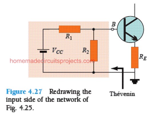
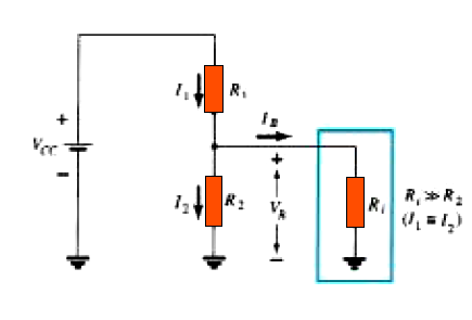
The input side of the network might be replicated as shown in Fig. 4.27 for the dc analysis, with reference to the accompanying image.
Then, as shown below, the Thévenin equivalent network for the schematic on the left hand side of the BJT base B may be found:
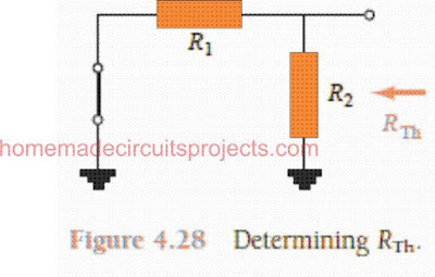
RTh: As seen in Fig. 4.28 below, an analogous short-circuit is used in place of the input supply points.

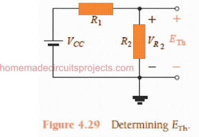
ETh: After applying the supply voltage source VCC back into the circuit, the open-circuit Thévenin voltage shown in Fig. 4.29 beneath is assessed as follows:
The next equation is obtained by applying the voltage-divider rule:

Then, using the Thévenin design as shown in Fig. 4.30, we assess IBQ by first using Kirchhoff's voltage law for the loop that runs in a clockwise orientation:
ETh - IBRTh - VBE - IERE = 0
As we are aware, IE = (β + 1)IB after replacing it in the loop above and determining out IB, we get:

Equation. 4.30
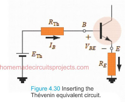
Although Eq. (4.30) appears to be somewhat distinct from the other formulas that have been established thus far, looking more closely reveals that the denominator is the result of base resistance + emitter resistor, which is reflected by (β + 1) and is undoubtedly very similar to Eq. (4.17) (Base Emitter Loop), whereas the numerator is simply a difference of two volt levels.
Following the calculation of IB using the equation above, the remaining values in the schematic may be found using the same technique as the emitter-bias network, as illustrated below:

Equation (4.31)
Working with a Real-World Example (4.7)
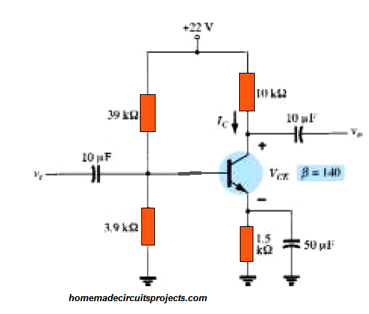
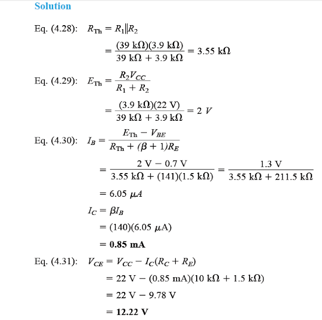
In the voltage-divider network Fig. 4.31 below, determine the DC bias voltage VCE and the current IC.
Figure 4.31: Example 4.7's beta-stabilized circuit.
Approximated Analysis
After learning the "exact method" in the previous part, we will now go over the "approximate method" for examining a BJT circuit's voltage divider.
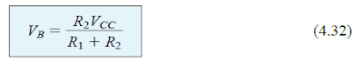
A BJT-based voltage-divider network's input stage could be illustrated as seen in figure 4.32 below.
The resistance It is possible to think of Ri as the resistance equivalent between the circuit's base and ground lines, and RE as the resistor between the emitter and ground.
You remember from our earlier discussions [Eq. (4.18)] that the equation Ri = (β + 1)RE explains the resistance replicated or expressed between the base and emitter of the BJT.
IB will be comparatively less than I2 if we assume a scenario in which Ri is much greater than the resistance R2 (keep in mind that current always seeks out and moves in the direction of least resistance), and I2 will then roughly equal I1.
I1 = I2, and R1 and R2 might be considered series elements if the estimated value of IB is practically zero with respect to I1 or I2.
A partial-bias circuit for estimating the estimated base voltage (VB) is shown in Figure 4.32.
Using the voltage-divider rule network, the voltage across R2, which was initially the base voltage, may be calculated as follows:
Given that Ri = (β + 1)RE ≅ βRE, the following equation determines the condition that verifies the feasibility of using the approximation approach:
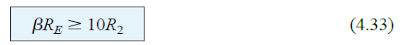
In other words, the approximation analysis may be implemented with maximum precision if the value of RE times the value of β is at least 10 times the value of R2.
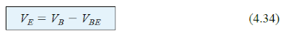
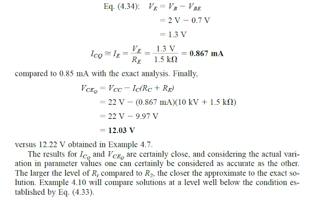
Following the evaluation of VB, the following equation might be used to calculate the VE magnitude:
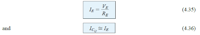
whereas the following formula may be used to get the emitter current:
The following formula may be used to get the voltage from collector to emitter:
VCE = VCC - ICRC - IERE
But because IE ≅ IC, we have the formula that follows:
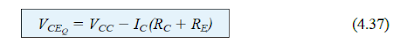
Notably, the element β is absent from all of the computations we performed using Eqs. (4.33), 4.37, and 4.33, and IB is not being utilized.
As a result, the Q-point (as determined by ICQ and VCEQ) is not reliant on the value of β. This is demonstrated in Practical Example (4.8):
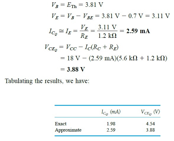
Together, we will compare the ICQ and VCEQ solutions by applying the analysis to our previous Figure 4.31 applying an approximation technique.
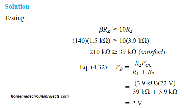
At this point we see that the VB level is the same as the ETh level, which was assessed in our earlier example 4.7. In other words, RTh, which is in charge of distinguishing ETh and VB in the precise analysis, influences the discrepancy between the approximate and exact analyses.
Going forward
Next, Example 4.9
To determine the difference between the ICQ and VCEQ solutions, we are going to perform the exact analysis of Example 4.7 if β is reduced to 70.

The answer
The following example may only be used to assess the extent to which the Q-point may shift if the magnitude of β is lowered by 50%, not to compare precise and approximate techniques. The values for RTh and ETh are identical, which means that
The following is obtained by tabulating the findings:
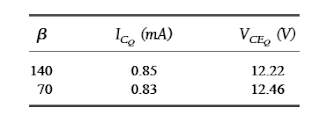
We can clearly see from the above data that the circuit is not very sensitive to changes in β values.
The values of ICQ and VCEQ are nearly same, although the β magnitude has been drastically decreased by 50%, from 140 to 70.
Next, Example 4.10
Combining the precise and approximate procedures, analyze the results to determine the values of ICQ and VCEQ for the voltage-divider network seen in Fig. 4.33.
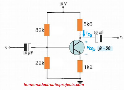
Although the conditions in Eq. (4.33) might not be met in the current situation, the results could aid us in determining how the solution differs when the criteria of Eq. (4.33) are ignored.
Example 4.10's voltage-divider network is shown in Figure 4.33.

Solving using Exact Analysis:
Applying Approximate Analysis for Solving:
We may observe the distinction between the outcomes obtained using accurate and approximate approaches from the assessments above.
According to the data, VCEQ is 10% lower and ICQ is around 30% higher for the estimated technique. Even while the findings are not exactly the same, they are also not very different given that βRE is only three times larger than R2.
stated that in order to guarantee the highest level of similarity between the two analyses, we would mostly depend on Eq. (4.33).
Leave a Reply