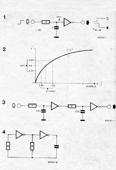
There are many occasions when a switching delay is required. One way of achieving this is to use an RC network and an inverter (see figure 1). This is quite practical and obvious as there are nearly always some gates "left over’ in a circuit. Unfortunately, every electronic component has a definite tolerance and so it is vir- tually impossible to determine the delay precisely in advance. However a considerable improvement can be achieved by connectingtwo inverter/ RC networks in series as shown in figure 3. ` The nominal threshold voltage of the inverter in figure lis half the supply voltage and has a tolerance of 1 30%. Figure 2 shows the signal input to the gate. If this input is between Us = 0.35 Ub and UC = 0.65 Ub the inverter may consider it either logic 'O' or ’1’! These voltages occur when a capacitor is charged through a resistor after a period of 0;43 1' and 1.051 respectively. (T is the time ` constant of the circuit and is equal to R x C). The nominal threshold voltage UC = 0.5 Ub is reached after a time of t = 0.69 T. s
lf the two inverters and RC networks of figure 3 are used, each RC net- work must produce the same delay, equal to half the total value of figure 1. The total delay will then be 1/2 x 0.43 T+ 1/2 x 1.05 T= 0.74 T at its worst case! This is a lot closer to the nominal value of 0.69 T.
The foregoing should make it clear f why the circuit of figure 4 gives such consistently reproducible results, Hovvever, for really satisfactory _ operation, Cll/IGS inverters must be used. The reason is that these gates have a threshold value of about half the supply voltage. Further, their output vi/ill always be either zero or the supply voltage. Schmitt triggers should not be used! lf the delay times using 4000 series CMOS are found to be too long the new 74HCXX series can be used. These are pin and function compatible to the 74LSXX series and just as fast!
