In this we learn how to make a simple opamp using a handful of transistors or BJTs, which will work quite like an opamp and can be configured like normal opamps but using transistors
How the Parts are Calculated
Intended for a power output of 20mW (RMS), the maximum output power will probably be 40mW as well as peak output current is going to be I^2*R =.04 and I(peak) = 32 mA. The negative peak of the output signal takes place whenever transistor Q3 is totally switched off, so the output voltage is only the consequence of a voltage divider 40 ohms and R4. In case the peak current is 32 mA, then the peak output voltage is going to be E=IR = .032*40 = 1.28 volts. Considering that the negative supply voltage is 3 and the peak load voltage is 1.28, you will have 3-1.28 = 1.72 volts throughout R4. Therefore, we want a resistor which lowers 1.72 at 32 mA or R4 = E/I = 1.72/.032 = 54 ohms, or 56 normal value.
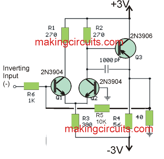
Second thing to consider was the base and collector currents for Q3. Since output voltage movement is well balanced, the peak voltage around R4 is going to be 3 + 1.28 or 4.28 and the current within R4 is going to be I= E/R = 4.28/56 = 76mA. The peak collector current of Q3 could subsequently be 76mA in addition 32 milliamps in the load or, 108mA in all. This appears slightly high for a 2N3906, perhaps some different transistor would be better.
Third thing to consider was the stable state DC current for the differential pair of transistors (Q1,Q2). The DC currents of Q1,Q2 needs to be fairly uniform (without any signal) to ensure that the two transistors hold close to equal DC currents. And this current needs to be relatively more than what exactly is required by Q3. The calculated hFE gain of the 2N3906 at 100mA was around 100, therefore the peak base current of Q3 need to be approximately 1 mA. The DC current for Q1,Q2 had been then decided to be around Three times better, or 3mA for each transistor (6 mA total). It may be bigger, however would certainly enhance battery drain.
Next thing seemed to be to sort out the common emitter resistor R3. Because the base of Q2 is at ground, the emitters will probably be around -700mV and the voltage throughout R3 will probably be 3-0.7 = 2.3, and the value of R3 is going to be E/I = 2.3/0.006 = 390 ohms. The total current in R3 will be 6mA, or 3mA per transistor Q1 and Q2.
Fifth action was going to designate a value to the Q3 e/b resistor (R2). In the symmetrical (no signal) state, Q3's base current is going to be around 0.5mA and the remaining current for R2 will likely be 3mA - 0.5mA = 2.5mA, therefore the resistor value could be R2=Vbe/.0015 = 0.7/.0025 = 280 ohms (270 standard value). Resistor R1 could have the same value and is accustomed to determine the DC current in Q1 which needs to be about 3mA, therefore the voltage around R1 should read about 810mV if everything is functioning correct.
The amplifier gain had been picked to become ten or (20dB) that describes the ratio of R5 to R6, or 1K and 10K. This helps make the input impedance around 1K because the inverting setup is utilized. For a greater input resistance, bigger resistor values could possibly be applied (10K 100K) etc. Or else you could possibly ground the 1K input resistor R6 and make use of the non-inverting input point (base of Q2) as a high impedance input.
Hints for making an opamp with transistors:
A smaller 1000pF cap had been included to restrict the bandwidth to approximately 100kHz and reduce oscillations. The value had been identified by experimentation.
The opamp circuit using transistors appears reasonably linear (reduced distortion) as pointed out in the scope picture listed below. The upper waveform is the ramp input from a function generator, and the bottom waveform is the inverted output of the op-amp having a 50 ohm load. Therefore, is in reality a graph of the increasing input ramp and dropping output ramp (2.25v p-p). Observe there exists a minor flex in the output line implying certain nonlinearity (disfigurement) however difficult to notice.
The DC offset at the output will probably shift negative as the battery voltage drops. This assessed around +50mV at full supply voltage and drifted negative to -150mV using the supply at +/- 2.5 volts. This is often remedied having a little realignment to R3. Reducing R3 increases the current in Q1/Q2 and transfer the DC offset positive, and visa versa. An additional strategy would be to substitute R3 with a constant current supply (1 additional transistor) which will conserve the DC offset close to zero as the supply voltage drops. However it probably would not be a 3 transistor opamp any longer. It might be a 4 transistor opamp.
Hi
I think Q3 is upside down
Emitter and collector must
Replaced
Is not it ?
Hi, you are right, Q3 must be turned upside down…sorry for the mistake.