This article teaches how to create a basic variable power supply circuit with the use of the 2N3055 transistor and a few additional passive elements. It comes with adjustable variable voltage and current features, completely customizable.
Key Features
1) The voltage can be adjusted to ranges of 0-30V, 0-60V, and 0-100V, and the current can be set from 500mA to 10 Amp according to the user's choice.
2) Short Circuit Protection is provided when installed on an appropriate heatsink.
3) Smooth without ripples, with a maximum of 1V peak-to-peak amplitude.
4) DC output is filtered and stabilized.
LED indicator for short circuit detection
6) Protected from overload
Overview
A power supply circuit lacking variable voltage and current control features cannot be deemed truly versatile under any circumstances.
This article describes a workbench power supply circuit that includes both variable voltage control and adjustable current control for overload protection.
Circuit Diagram
Circuit Description
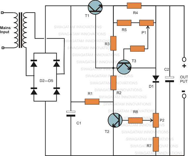
Examining the variable voltage current power supply circuit utilizing transistor 2N3055 shows that despite being a basic stabilized power supply, it effectively offers the desired functions. Voltage adjustments are achieved by manipulating preset P2 in a feedback loop involving components D1, R7, T2, and P2.
Including D1 ensures that the voltage can be reduced all the way to 0.6 volts, which coincides with the diode's forward voltage drop.
If a different minimum value is needed, the diode can be substituted with a zener diode with the specified value.
So in this variable power supply circuit with a 2N3055 transistor, the output range can be adjusted from 0.6 to a maximum of 40 volts, thanks to the transformer's 0 – 40 V capacity.
T3, P1, R5, and R4 are utilized in implementing the current control feature.
The maximum allowable output current is defined specifically by the value of R4.
P1 is adjusted to select the widest range within the value specified by resistor R4.
PCB Design
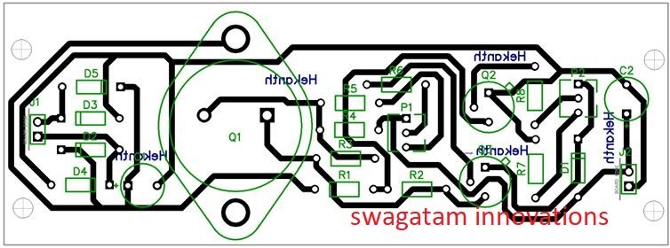
Parts List
| Component | Value/Specification |
|---|---|
| R1 | 1K, 5 Watt, wire wound |
| R2 | 120 Ohms |
| R3 | 330 Ohms |
| R4 | To be calculated using Ohm's Law |
| R5 | 1K5 |
| R6 | 5K6 |
| R7 | 56 Ohms |
| R8 | 2K2 |
| P1, P2 | 2K5 presets |
| T1 | 2N3055 |
| T2, T3 | BC547B |
| D1 | 1N4007 |
| D2, D3, D4, D5 | 1N5402 |
| C1, C2 | 1000 µF / 50V |
| Tr1 | 0–40 Volts, 3 Amp |
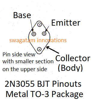
2N3055 Pinout Details
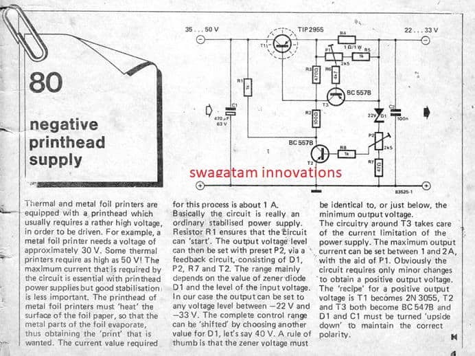
Transistor Power Supply Diagram depicted in the original diagram.
The design above was influenced by the circuit created and featured in the elektor electronics magazine by the elektor engineers.
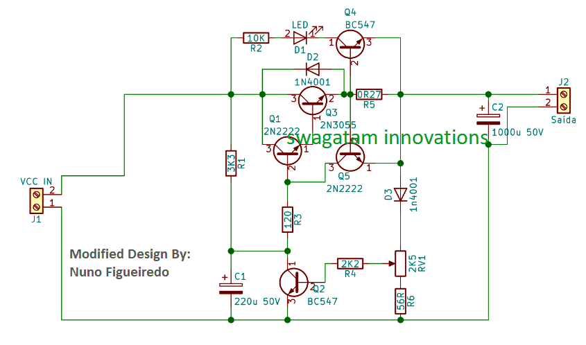
Design a Variable Power Supply with Simplified Circuit using 2N3055 and 2N2222 Transistors
The updated and streamlined layout can be seen in the diagram below:
The design features LED indication for over-current shut down.
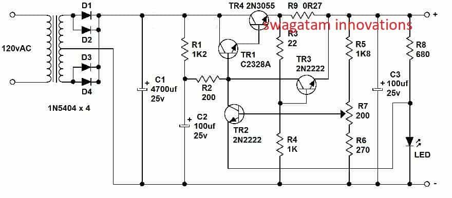
Presented below is a power supply design similar to the one referred by Mr. Collins for the viewer's evaluation.
2N3055 Regulator with Adjustable Voltage Range
The main features of the circuit include: broad output range from 0.1 to 50 volts, good load regulation of 0.005% at 0-1 amp, average line regulation of 0.01%, and minimal output disturbance less than 250 microvolts.
The wide range of output options is achieved using the CA 3130 integrated circuit, which can function with no difference between input and output voltages. Additionally, by incorporating T4 between the IC and the series pass transistor, it becomes possible to extend the output range even further.
The elevated level of amplification achieved allows for better control, and the T1/T2 Darlington pair provides sufficient current amplification. T3 functions as a controller for output current.
When P1 is turned completely counterclockwise, T3 limits to 0.6 amps. The limiting circuit deactivates when P2 is turned all the way to the right. The regulator circuit operates in a specific manner.
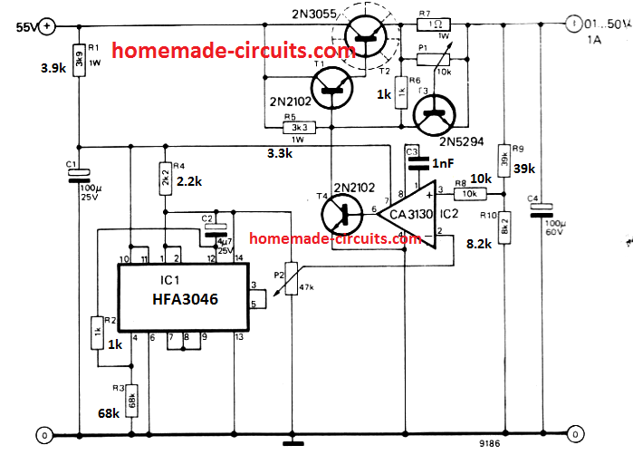
The IC CA 3130 compares the output voltage received by the non-inverting input to a reference voltage at the inverting input.
To prevent damage to the IC, a potential divider is used to lower the output voltage of the regulator.
The reference voltage is set by P2, a high-quality component, as any noise on its slider arm will likely affect the regulator output.
Another integrated circuit, known as HFA3046, compensates for the reference voltage changes caused by temperature fluctuations. The IC consists of 4 transistors utilized as diodes or zener and an additional transistor to reduce the output impedance of the reference circuit.
The reference IC also supplies a reduced voltage for powering CA 3130. The utilization of both ICs in the regulator stage is essential; removing IC1 could lead to the failure of IC2. Every transistor in the diagram needs to have a minimum breakdown voltage of 55 volts.
Variable power supply with high current capabilities.
In this circuit for a high current linear power supply, a 2N5686 transistor is utilized instead of 2N3055 to enable a minimum current delivery of 10 amps. The preset P3 can be adjusted to set a current range of 10 amps.
Constructing the power supply is relatively simple in itself. An IC LM329 generates a constant voltage reference of 6.9 V.
P4 is a potentiometer that is used to measure the output voltage with the help of a preset potential divider P2-P4-R2. IC1 and T1 form the power stage of the circuit and function similarly to an operational amplifier for positive voltages (negative voltages are not important in this context).
An op amp, P1, R5, and R6 are combined to create this non-inverting amplifier. This suggests that the voltage at the midpoint of P4 is directly related to the voltage measured across the output points.
Potentiometer P1 adjusts the maximum output voltage, whereas P2 is utilized to establish the minimum output voltage of the power supply.
Preset P3 is employed to establish the highest current threshold for the output.
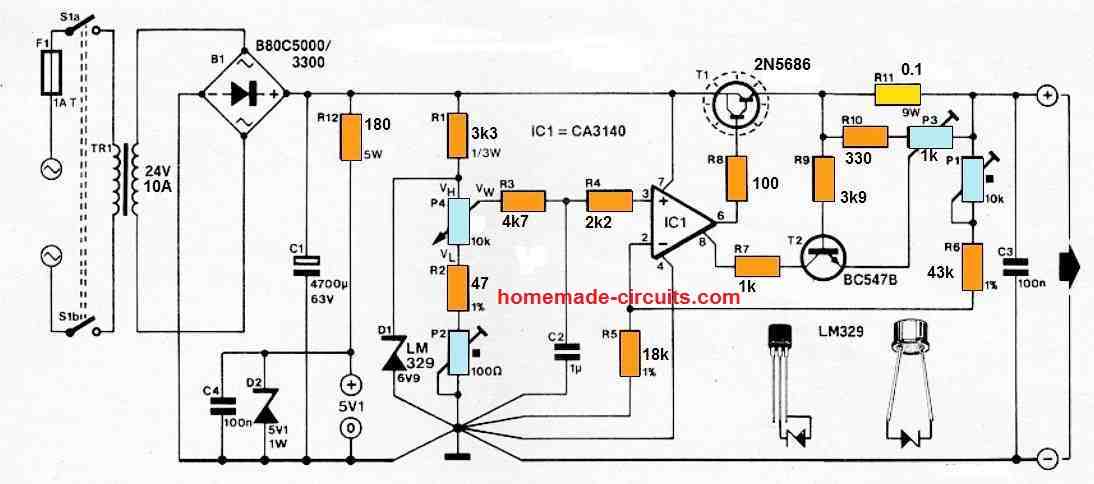
This is achieved by converting the output current to a voltage using R11. When the voltage, regulated by P3, is at a high enough level to activate T2, the current regulation through IC1's strobe input takes precedence over the circuit's voltage regulation. The current can be adjusted anywhere from 0.8 A to 10 A, with the adjustments of the controls determining the maximum.
To avoid T1 from getting damaged and excessive dissipation, the current should not exceed 25A when the power supply output is short-circuited. Setting up the circuit is simple. Start by setting P4 to its maximum resistance and let Z1 and IC1 reach their usual operating temperatures after approximately one minute. Then, modify P1 in order to achieve a 25 V output voltage.
In the end, adjust P2 so that it produces a 250 mV output voltage by adjusting P4 to the lowest resistance setting. The intentional choice of a minimum output voltage of 250 mV ensures that each component can consistently operate within the linear range of its characteristics. A couple of reminders: the earth lines must follow the schematic and T1 must be attached to a 1.5 K/W heat sink.
Leave a Reply