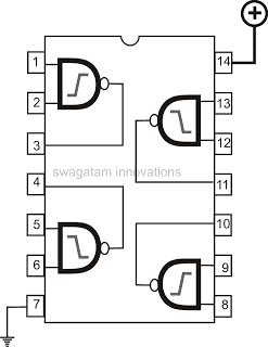
The following tutorial teaches us the way to implement the IC 4093's NAND gates, or any additional equivalent integrated circuit.

About IC 4093
Despite its simple features and specs, the IC 4093 offers a number of practical applications. It is made up of a few basic building blocks that may be used for a wide range of applications and customized to suit individual tastes.
The IC 4093 appears to be a fairly typical dual in line IC from the outside.
It contains four CMOS blocks incorporated inside within its packaging and has fourteen pins.
These blocks are known as gates; in this context, they are referred to as NAND gates.
You'll find nothing complex regarding the IC 4093's NAND gates; they are easy for one to comprehend and use.

Although these gates are contained inside a package rather than being separate components like transistors, you may think of them as an electrical component with a few inputs and a single output.
But as compared to linear devices like transistors, the gates described above have completely different properties.
Simply expressed, the gates are designed to respond to certain combinations of input voltage instructions by producing certain sets of output voltages.
Think about a single NAND gate, which has one output and two inputs.
A negative voltage is obtained at the output pin when you supply a positive voltage to both inputs.
A positive voltage is obtained at the output by applying ground or negative voltages to both inputs.
When opposite voltage levels are applied to the input pins, the output remains positive and is unaffected.
The data, which is often provided in the form of truth tables, informs us of the logical quality of the gate, specifically for a NAND gate.
It is crucial to remember that the inputs must never be left open and must constantly be applied with certain voltage levels.
Absolute Maximum Rating
To prevent irreversible damage to the IC 4093, the accompanying ratings show the highest and lowest values that should never be exceeded when operating the device.
| Parameter | Description | Value/Range |
|---|---|---|
| VDD | Supply voltage at pin #14 | -0.5 to +22 V |
| VI | DC input voltage | -0.5 to VDD + 0.5 |
| II | DC input current | ±10 mA |
| PD | Power dissipation per package | 200 mW |
| PD | Power dissipation per output transistor | 100 mW |
| Top | Operating temperature | -55 to +125°C |
| Tstg | Storage temperature | -65 to +150°C |
How to Use
Utilization of the IC 4093 is dependent upon the truth table functions and the way the gate outputs react to gate input logics or voltages.

Although an electrical circuit's output pin is typically utilized to initiate the subsequent stage, it has no the significance and, if left open, won't harm the IC.
Nonetheless, the voltage provided to the gate inputs must never be higher than the IC's supply voltage, which must also fall within the designated range, often between 2 and 15 volts.
Depending on CMOS gates, undefined voltage values fall between 0.75 and 2.5 volts. Everything under 0.75 is regarded as a logic 0 or a logic low, while anything above 2.5 is regarded as a logic 1 or logic high.

What is Schmitt Trigger
Despite the fact that the IC 4093 functions just like any other NAND gate and even has similar truth table numbers, it is known as a Schmitt trigger. Why?
The reason for this is that the IC 4093 gate's output reaction to an input signal lags with a slight time delay, ensuring that the output is only ever impacted by real input signals and never by errant or inadvertent input signal changes. The IC's inherent hysteresis effect characteristic is what causes this function.
Assume, for instance, that the gate input receives a very brief transient pulse, perhaps just below the threshold of a real input logic pulse level.
Because of the short delay in the output response, the 4093 Schmitt trigger gates cannot pick up these pulses and will instead wait until the signal is determined to be over the appropriate thresholds. The gate's output is going to remain steady and unaltered in this circumstance.
Only when a real input pulse is detected—which is continuously high or low during the gate's hysteresis delay margin—will the gate output status modification.
Application Circuits
We'll look at how the IC 4093 may be used to construct a few modest application circuits in the next section.
The first circuit below is a basic circuit for a twin LED flasher. By utilizing only three of the IC's gates, both of the LEDs sequentially flicker. Let's examine this explanation in greater detail.
Alternate LED Flasher Circuit

Above is a basic circuit for a dual alternate LED flasher that uses a single IC 4093. The P1 pot allows you to control the frequency or flashing speed of the LEDs, which will alternately flash.
The supply voltage and the quantity of LEDs utilized will determine the R2 and R3. The formula below can be used to set these:
R = supply voltage - total LED forward voltage / LED current
The forward voltage of a typical single LED may be estimated to be 3.3V, 6.6V for two in series, and so on.
A little running LED Light effect
As seen in the accompanying graphic, a single 4093 IC may provide a tiny and portable running LED effect.
The capacitors C1, C2, and C3, as well as the resistors R1, R2, and R3, will determine how quickly the linked LEDs appear to be chasing one another in a circle.
The LEDs' operating frequency may be changed by varying these components.

Leave a Reply